
@nuclear_kote

-
Электроника
-
Схемотехника
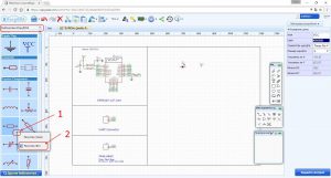
Жму Library-> Нахожу нужный компонент ->жму редактировать->сохраняю. А как теперь его добавить на схему?
-
Вопрос заданболее двух лет назад
-
972 просмотра
Комментировать
Подписаться
1
Простой
Комментировать
Решения вопроса 0
Пригласить эксперта
Ответы на вопрос 0
Ваш ответ на вопрос
Войдите, чтобы написать ответ
Войти через центр авторизации
Похожие вопросы
-

-
Электроника
- +1 ещё
Простой
Подключение 4-х канального усилителя 2-м канал 4-х канальной магнитолы?
-
1 подписчик -
16 часов назад
-
55 просмотров
1
ответ
-
-
-
Железо
- +3 ещё
Простой
Как запустить жесткий диск 3.5?
-
1 подписчик -
23 часа назад
-
126 просмотров
5
ответов
-
-
-
Arduino
- +1 ещё
Средний
Правильно ли подключен процессор ардуино?
-
1 подписчик -
07 февр.
-
81 просмотр
2
ответа
-
-
-
Железо
- +3 ещё
Простой
Как сделать выносную кнопку включения пк из переключателя от механической клавиатуры?
-
1 подписчик -
06 февр.
-
150 просмотров
3
ответа
-
-
-
Электроника
- +1 ещё
Средний
Как подобрать аудио-трансформатор для небольшого динамика 0.5W 8Ohm?
-
2 подписчика -
01 февр.
-
123 просмотра
3
ответа
-
-
-
Электроника
- +1 ещё
Простой
Есть ли смысл ремонтировать проектор?
-
2 подписчика -
31 янв.
-
110 просмотров
0
ответов
-
-
-
Электроника
- +1 ещё
Простой
Блок зарядки 61w борохлит?
-
1 подписчик -
29 янв.
-
78 просмотров
0
ответов
-
-
-
Электроника
- +2 ещё
Средний
Как подключить домофон к умному дому?
-
10 подписчиков -
28 янв.
-
510 просмотров
2
ответа
-
-
-
Электроника
- +2 ещё
Простой
Как подключить пульт от радиоуправляемой машинки к моторчику 12в?
-
1 подписчик -
26 янв.
-
153 просмотра
2
ответа
-
-
-
Электроника
Простой
Что можно сделать с NC контактами?
-
1 подписчик -
25 янв.
-
101 просмотр
2
ответа
-
-
Показать ещё
Загружается…


Вакансии с Хабр Карьеры
Инженер-программист C# (1,2 категории)
НПО «СПАРК»
•
Санкт-Петербург
от 80 000 ₽
Системный аналитик (внутренняя безопасность)
Сбер
•
Москва
от 200 000 до 250 000 ₽
Программист Python/Python Developer
Нуматех
от 150 000 ₽
Ещё вакансии
Заказы с Хабр Фриланса
Дописать Приложение на GO
09 февр. 2023, в 13:28
777 руб./за проект
Работы над сайтом
09 февр. 2023, в 13:09
5000 руб./за проект
Сверстать страницу для laravel
09 февр. 2023, в 13:08
1000 руб./за проект
Ещё заказы
Минуточку внимания
Присоединяйтесь к сообществу, чтобы узнавать новое и делиться знаниями
Зарегистрироваться
Это пошаговое руководство с большим количеством скриншотов рассчитано, в первую очередь на тех, кто только начинает знакомится с электроникой, либо не использовал EasyEDA ранее, однако, надеюсь, что и профи смогут почерпнуть что-то полезное. Все скриншоты уменьшены для удобства чтения статьи с мобильных устройств, но кликабельны для отображения в бОльшем размере. Это не перевод оригинального туториала, а лишь скромная попытка автора поделиться своими собственными первыми шагами в освоении EasyEDA.
Какие возможности предоставляет EasyEDA
Чем еще примечателен сервис EasyEDA
С чего начать работу в EasyEDA
Переключение интерфейса на русский язык в EasyEDA
Создание нового проекта в EasyEDA
Создание новой схемы в проекте EasyEDA
Основные приемы редактирования схем в EasyEDA
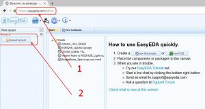
Добавление компонентов в схему EasyEDA
Различные подходы в проектировании схем
Соединение компонентов схемы
Сохранение схемы в EasyEDA
Как поделиться своим проектом с другими
Как скопировать чужой публичный проект себе в EasyEDA
Предоставление доступа к проекту в EasyEDA
Заключение
EasyEDA – это кроссплатформенный комплекс, предназначенный для разработки электрических принципиальных схем, автоматизированной разводки печатных плат и предоставляет возможность осуществить заказ на изготовление ваших плат. Возможно, что вас заинтересует и симулятор электронных схем, который тоже входит в список бесплатных услуг, предоставляемых EasyEDA. В состав EasyEDA входит:
- редактор электрических схем, компонентов и готовых модулей с обширной автоматически обновляемой библиотекой, содержащей сотни тысяч комплектующих, символы компонентов как в американском, так и в привычном нам, европейском форматах. Вы можете как создавать собственные компоненты и модули, так и редактировать существующие
- трассировщик, редактор топологии (проводящего рисунка) печатных плат
- симулятор схем (модули ESP8266, конечно же, не поддаются симуляции), движок симулятора от ngspice
- просмотрщик файлов формата Gerber
- изготовление печатных плат по демократичным ценам (9,8$ за 10шт. +доставка в РФ — 6,6$ (получается 1,64$ за 2-х стороннюю плату размером 50×50мм с учетом доставки — для меня уж лучше подождать доставку, чем возиться с химией, да и качество ЛУТ уже не устраивает)
Заказ плат на EasyEDA не является обязательным условием использования этого сервиса и вы вполне можете либо не заказывать платы вообще, либо заказать их у любого изготовителя по вашему выбору (есть бесплатный экспорт плат в формате Gerber).
Сервис бесплатный (техподдержка отвечает в течение 48 часов по email на английском), с возможностью получить более быструю техподдержку (время ответа до 24 часов по электронной почте, и техподдержка по телефону) и скидку до 10% на заказ плат при использовании платной подписки.
Кроме того, представитель EasyEDA обещает отвечать на вопросы наших пользователей (к сожалению, только на английском языке), касающихся выполнения заказов на изготовление плат на нашем форуме в специальном разделе.
Бесплатный тариф не накладывает ограничений на размеры платы, количество слоев или контактных площадок.
Для подавляющего большинства пользователей вполне будет достаточно возможностей, предоставляемых на бесплатном тарифе. Более подробно с тарифами вы можете ознакомиться здесь.
В настоящий момент EasyEDA русифицирован примерно на 90%, что позволяет вполне комфортно работать людям, предпочитающим локализованные версии. Неполная русификация, видимо, объясняется тем, что перевод на русский язык был осуществлен некоторое время назад и новые, либо переделанные фичи оказались на английском. Для меня это даже хороший знак — это показывает, что сервис не умирает и хозяева его не бросили, раз он развивается. А десяток-другой английских фраз мы можем и потерпеть.
Очень важной считаю возможность использования сервиса в коммерческих проектах и совместной работе над одним проектом командой разработчиков, которая предоставляется даже на бесплатном тарифе. Можно предоставить и read-only доступ, например, студент может предоставить доступ на просмотр своего проекта своему преподавателю, оставляя свой проект недоступным для других пользователей.
Количество проектов (как приватных так и публичных) на бесплатном тарифе не лимитируется, что меня тоже очень порадовало.
Форум проекта живой, и на нем реально получить помощь (жаль, что нет русскоязычной техподдержки). Разработчики отвечают на багрепорты и предложения по расширению функционала (на английском и китайском языках).
Меня впечатлила возможность вставлять в свои сообщения на форуме скриншоты прямо из буфера обмена (эта фича работает только в хроме), что очень удобно для общения с техподдержкой.
Чем еще примечателен сервис EasyEDA
EasyEDA — это не программа на вашем компьютере, а облачный сервис в интернете, а это значит что вы можете его использовать на компьютере с любой операционной системой. Соответственно, для работы не нужно устанавливать какие-либо программы и библиотеки — необходим только браузер и доступ в интернет (разработчики EasyEDA обещают выпустить программу для работы оффлайн, которая не будет требовать подключения к сети интернет).
Ваши проекты будут хранится в облаке (бесплатно) и вы сможете получить к ним доступ из любой точки земного шара с любого компьютера или даже смартфона или планшета.
EasyEDA работает в большинстве популярных браузеров, но максимальные возможности вы получите, если будете использовать Google Chrome. Разумеется, что Firefox тоже поддерживается (кстати, скриншоты к этой статье я делал как в хроме, так и Firefox). На Safari существуют определенные проблемы, поэтому инженеры EasyEDA рекомендуют пользователям MAC и iPhone использовать хром при работе с их сервисом.
Скорость прорисовки схем и плат в браузере меня тоже впечатлила — даже большие проекты прорисовываются без ощутимых тормозов. Разработчики сообщают, что максимальная скорость рендеринга обеспечивается в Chrome, а Firefox будет чуть медленнее, но показывает вполне приемлемые результаты.
С чего начать работу в EasyEDA
Начать лучше с регистрации, чтобы созданный проект был привязан к вашему аккаунту и никуда не потерялся. Регистрация проходит по типичному сценарию.
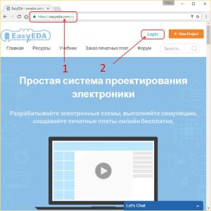
Переходим на сайт EasyEDA
Переходим на русскоязычную версию сайта EasyEDA и жмем кнопку Login (я уже писал, что перевод на русский язык осуществлен примерно на 90%)
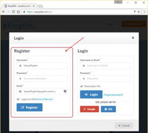
Регистрационная форма EasyEDA
и заполняем регистрационную форму слева своими данными: ваш ник на сервисе, пароль не менее 6 символов и ваш адрес электронной почты. Галочка должна быть отмечена и означает что вы соглашаетесь с условиями использования сервиса. Term of Service на русский не переведено, но я почитал — там все стандартное: они никому не передают ваши данные, вам будет показана реклама и бла-бла-бла. Как все заполните — жмите Register. Понятно, что в последующем, для входа на сервис, вы заполняете уже форму справа теми же данными, что и при регистрации. Вход через Google работает с глюками, в настоящее время использовать не рекомендую. QQ — это китайский мессенджер, так что если вы в нем не зарегистрированы, то можете не обращать внимания.
Практически сразу на почту приходит письмо, в котором нужно кликнуть по ссылке для подтверждения вашего адреса электронной почты.
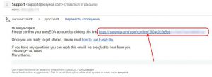
Письмо с подтверждением адреса электронной почты в EasyEDA
На этом этапе все — регистрация завершена.
Переключение интерфейса на русский язык в EasyEDA
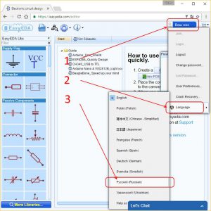
Переключение интерфейса EasyEDA на русский язык
Переключения интерфейса EasyEDA на русский язык осуществляется непосредственно в редакторе. Можете перейти по прямой ссылке в редактор, кликнуть в правом верхнем углу по своему нику, в появившемся меню, в самом низу, выбрать Language, затем Russian
Создание нового проекта в EasyEDA
Проект в EasyEDA — это совокупность схем и данных о разметке вашей платы. Так что если вы планируете даже просто нарисовать схему, то вы должны создать новый проект и уже в нем создать новую схему. Это может показаться лишним действием, однако приучит вас к порядку раскладывать все по папочкам. У вас же не лежат все документы на рабочем столе без папок? Или все таки да 
Новый проект можно создать «с нуля» или склонировать у кого-то уже существующий (как это сделать будет показано ниже). Также кто-то может предоставить вам доступ к своему проекту для совместной работы.
Создание вашего первого проекта в EasyEDA
Для создания вашего первого проекта «с нуля» нужно перейти в редактор и там создать новый проект кнопкой слева вверху. В дальнейшем вы можете создавать новые проекты прямо с главной страницы EasyEDA.
Создание нового проекта в EasyEDA
Далее вам предлагается ввести название проекта и указать: будет ли ваш проект публичным (проект будет доступе в поиске и кто угодно сможет его склонировать себе в редактор и производить над копией любые действия), либо ваш проект будет приватным и посторонние не получат к нему доступа до тех пор, пока вы этого не захотите. Публичность/приватность проекта можно менять в последующем неограниченное количество раз.
Задайте подробное описание вашего проекта в поле Description.
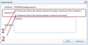
Выберите тип вашего проекта: приватный или публичный
Создание новой схемы в проекте EasyEDA
Создадим новую схему в нашем проекте — это можно сделать «с нуля» (ссылка справа на скриншоте), из шаблона (ссылка слева) или из внешнего файла (ищите импорт в меню). Тут вас ожидает приятный сюрприз: в системе уже есть шаблон схемы с минимальной обвязкой для модуля ESP8266 (ссылка слева на скриншоте). Вы можете создавать собственные шаблоны для последующего быстрого старта проектирования однотипных схем, что может оказаться весьма полезным.
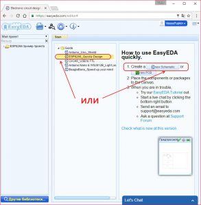
Создание новой схемы в EasyEDA
При создании новой схемы по правой ссылке, вы создаете схему не совсем «с нуля», как я вам сообщил выше. Вам будет предложено нарисовать новую схему в рамке, по буржуйским стандартам
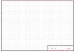
Новая схема в буржуйской рамке в EasyEDA
Возможность сделать рамку по ГОСТу, я думаю тоже есть, если самому нарисовать для нее собственный шаблон и начинать каждую новую схему уже с него. Может быть это уже кто-то и сделал, а вам осталось лишь «форкнуть» этот проект.
Схемы и библиотеки в проект можно импортировать из файлов на вашем компьютере, поддерживаются популярные форматы:
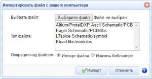
Импортирование схем и библиотек в EasyEDA
Мы, для примера, создадим новую схему из шаблона для ESP8266.
Основные приемы редактирования схем в EasyEDA
В редакторе схем EasyEDA отсутствуют полосы прокрутки (как горизонтальная, так и вертикальная). Вот так — совсем их нет (хотя в оригинальном туториале они присутствуют на скриншотах, значит были в предыдущих версиях движка). Если вы знаете как их включить сейчас — дайте мне знать, вдруг пригодится. Сначала я нашел отсутствие полос прокрутки очень неудобным, но быстро привык и теперь не замечаю их отсутствия.
Вы можете передвигать всю схему или только один выбранный компонент стрелками на клавиатуре. Мне показалось более удобным перетягивать всю схему мышью, зажав правую кнопку.
Мне очень понравилось плавное стократное (10000%) масштабирование схемы. Четко прорисованная, во всех деталях векторная графика масштабируется без потери качества. Впечатляет, что это реализовано прямо в браузере — респект разработчикам.
Масштабирование «по ширине листа», как в MS Word, можно сделать через верхнее меню, как мы привыкли, или нажатием горячей клавиши K в английской раскладке
Масштабирование (zoom) в EasyEDA
Увеличение любой области происходит легко: нужно сначала навести на эту область указатель мыши и прокрутить колесико скроллинга мыши вперед. Аналогично и уменьшение.
Добавление компонентов в схему EasyEDA
Подключим к ESP8266 светодиод. В качестве шпаргалки воспользуемся замечательным наглядным пособием Arduino Basic Connections — подключение всего в картинках v 2.0 Если вы новичок и еще не видели этот документ, то рекомендую сделать его вашей настольной книгой, чтобы избежать множества граблей, которые подстерегают начинающих радиолюбителей. Также хочу вам сообщить, что и ESP8266 и ATMEGA на Arduino являются микроконтроллерами и принципы подключения к ним периферии одни и те же, поэтому вы можете смело использовать рекомендации по Arduino для ESP8266, при этом не забывайте о том, что:
- Arduino бывают как 5-ти вольтовые, так и 3.3, а ESP8266 только 3,3
- Порты Arduino выдерживают ток до 40мА, а ESP8266 — только 12мА
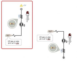
Подключение светодиода к выходу микроконтроллера
Возьмем из шпаргалки левый вариант, где мы видим, что для подключения светодиода нам нужен резистор и питание. При низком уровне на выходе GPIO светодиод будет включаться, а при высоком выключаться.
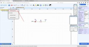
Скопируем элемент VCC из левой части схемы: левый клик мышью на элементе (не промахнитесь — вам нужна и надпись VCC и «частичка провода»), затем Копировать на панели инструментов и там же Вставить — эта процедура абсолютно аналогична действиям в обычном текстовом редакторе. Вставляемый элемент «прилипнет» к указателю мыши и вы вставляете его в правую часть схемы в свободное место кликом мыши.
![]()
Копирование и вставка в EasyEDA
Добавим резистор из Библиотеки EasyEDA
Выбираем привычный нам «европейский» символ компонента в EasyEDA
Различные подходы в проектировании схем
Сейчас мы должны подключить все это к одному из GPIO нашего модуля ESP8266 и тут можно пойти разными путями. Можно сделать по-старинке и соединить на схеме наши светодиод и резистор с выходом GPIO модуля на левой части схемы — именно так раньше и делали (многие продолжают делать так и сейчас, и не только в России). Получаются вот такие схемы:
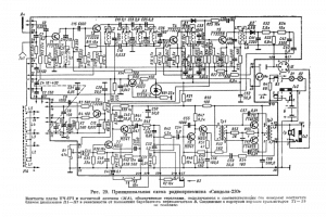
Схема радиоприемника Спидола-230
Но из зарубежья к нам пришло новое веянье — схемы, оформленные по-другому:
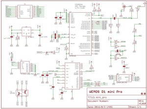
Схема Wemos D1 mini PRO 128Mbit (16 Мегабайт)
Такие схемы оформлены более модульно, не загромождены множеством соединительных линий от края до края. Соединение модулей производится через именованные электрические связи (проводники) с соответствующей маркировкой. Такие схемы менее привычны и некоторые радиолюбители считают, что они не позволяют увидеть сразу все детали. Попробуйте ответить на вопрос: какие элементы подключены к VCC на этой схеме? Можно легко упустить из виду какой-то модуль. Однако, если вы планируете выходить на международный рынок — не обязательно продавать что-либо, даже если вы просто размещаете свой проект в публичный доступ, то имеет смысл задуматься над выбором, и, возможно, сделать схему в современном виде, общепринятом в международном сообществе. Однако, это остается, безусловно, на ваше усмотрение.
Соединение компонентов схемы
Для соединения светодиода с одним из выводов ESP8266 (например, GPIO2) нужно перейти из режима отображения набора атрибутов элемента в режим Менеджер разработки

Кнопка перехода в режим менеджера разработки в EasyEDA
В менеджере (справа) нужно найти группу Nets и в ней GPIO2
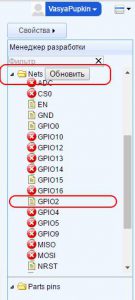
Выбор проводника (цепи) в EasyEDA
при этом в левой части вашей схемы GPIO2 на ESP8266 станет выделен красным цветом — его нужно скопировать и вставить в правую часть схемы.
Осталось только соединить элементы между собой — для этого просто тянем за край контакта и соединяем линию со следующим элементом. В результате у вас должно получиться следующее:
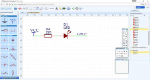
Схема подключения светодиода к ESP8266
Сохранение схемы в EasyEDA
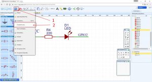
Сохранение схемы в EasyEDA
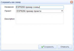
Сохранение схемы в EasyEDA
Как поделиться своим проектом с другими
Если вы сделали публичный проект, то сможете им поделиться с другими
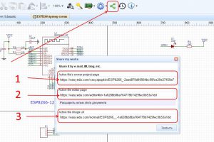
Как поделиться проектом в EasyEDA
Начнем снизу: третья ссылка ведет на PNG файл вашей схемы — вы можете вставлять эту ссылку на форумах, посылать ее по электронной почте, вставлять в сообщения в социальных сетях. Вот ссылка на наш демо проект.
Вторая ссылка предназначена лично для вас — вы можете поместить ее в закладки браузера для быстрого перехода в режим редактирования этой схемы.
Самая верхняя, первая ссылка ведет на страницу проекта. Вот так выглядит наш проект для других пользователей
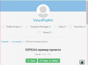
Публичный проект в EasyEDA
Как скопировать чужой публичный проект себе в EasyEDA
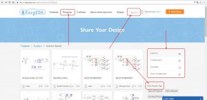
Поиск публичных проектов в EasyEDA
В разделе Ресурсы вы найдете множество публичных проектов, компонентов и модулей, которые вы можете скопировать себе, внести собственные правки и использовать в дальнейшем. На момент написания статьи поиск по проектам не работает, разработчики это уже знают и обещают исправить в ближайшее время (поиск по модулям и компонентам работает). Вы можете пользоваться поиском по популярным тегам (на скриншоте проекты с тегом Arduino Based)
Любой публичный проект вы можете скопировать себе («форкнуть») и он станет доступен для редактирования в вашем списке проектов в редакторе
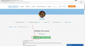
Как форкнуть публичный проект в EasyEDA
Публичный проект уже в редакторе
Предоставление доступа к проекту в EasyEDA
По умолчанию все ваши проекты будут приватными (напоминаю, что в EasyEDA, в отличии от других, не существует ограничения на количество приватных проектов). Для совместной работы над проектом вы можете предоставить доступ своему коллеге (коллегам). Вы можете предоставить доступ только для чтения (read-only) или полный (read/write) конкретному пользователю, для этого нужно кликнуть правой кнопкой мыши по названию проекта и ввести адрес электронной почты, на который зарегистрирован аккаунт EasyEDA вашего коллеги.
Предоставление доступа к проекту EasyEDA
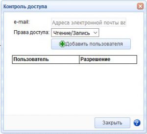
Предоставление доступа к проекту конкретному пользователю в EasyEDA
Заключение
Эта статья получилась слишком большой и я искренне благодарен тем, кто смог дочитать ее до конца. Даже в этом объеме мне не удалось рассказать о многих интересных возможностях EasyEDA. Возможно, это получится в следующих материалах.
В целом, впечатление от EasyEDA у меня сложилось очень положительное, несмотря на некоторые недостатки, которые меня огорчили. Я вспоминаю те времена, когда я начал осваивать DeepTrace, и потратил намного больше времени на свою первую схему. Здесь же все оказалось много проще, при достаточно широких возможностях. Так что я плюсую EasyEDA.
Мне импонирует дух open source, которым пропитан сервис EasyEDA — это и публичные проекты и легкость их использования и открытый формат файлов выгрузки проектов, о котором мне не удалось рассказать в этой статье. Этакий гитхаб, только не для программ, а для плат. Кстати, поддержка контроля версий плат была бы очень кстати
P.S.
Не скрывая сообщаю, что EasyEDA оказали поддержку нашему сайту и форуму (частично компенсировали мои личные расходы на VDS на котором для вас работают этот сайт и форум), и, в качестве благодарности, я разместил ссылки на сервис EasyEDA на сайте и форуме esp8266.ru. Могу вас заверить, что данный факт никоим образом не повлиял на объективность данного материала и какой-либо другой информации, размещенной у нас о сервисе EasyEDA.com
Ваш IoT евангелист, Виктор Бруцкий aka 4refr0nt.
Обсуждение этой статьи на нашем форуме
EasyEDA
При проектировании электронных устройств для домашнего или коммерческого использования нет необходимости в приобретении сложных систем автоматизированного проектирования.
В этом руководстве, я подробно расскажу про систему, понравившуюся мне, под названием EasyEDA.
EasyEDA — веб-среда для автоматизированного проектирования электронных устройств предназначенный, как для студентов-энтузиастов, так и профессионалов.
В основе EasyEDA лежит облачный сервис, который производит все вычислительные операции за счет мощных компьютеров расположенных в Китае. Таким образом, скорость выполнения задач зависит не от характеристик вашего компьютера, а только от скорости интернет-соединения. Также сервис имеет десктопный клиент, который немного упрощает и ускоряет работу, но все операции так же выполняются через облако.
EasyEDA предоставляет широкий спектр возможностей, например: редактор схем электрических принципиальных, редактор печатных плат, автотрассировка печатных плат, просмотровщик печатной платы в 3D, создание файлов для производства (Gerber) печатной платы, возможность моделирования схем электрических принципиальных, экспорт в BOM (такая своеобразная спецификация) и многое другое.
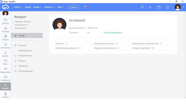
Центр пользователя в EasyEDA
Перед созданием проекта необходимо зарегистрироваться в центре пользователя. Для этого в правом верхнем углу жмем Зарегистрироваться.
В модальном окне проходим стандартную процедуру регистрации, вводим: имя пользователя, электронную почту, пароль. Также вход можно осуществить через аккаунт Google.
После подтверждения электронной почты и входа в аккаунт, перейдем в центр пользователя выполнив простые действия, как показано на рисунке:
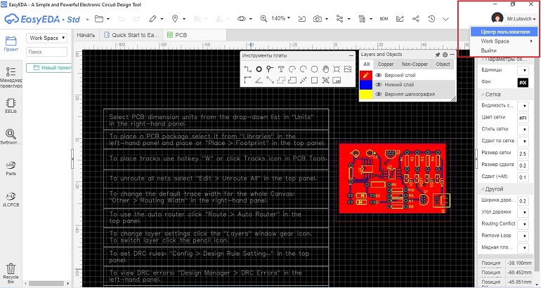
Центр взаимодействия можно описать как социальную сеть, где можно делиться своими проектами электронных устройств, библиотеками компонентов и корпусами с другими участниками среды. Ваши проекты могут быть, как приватными, которые можете видеть и редактировать только вы, так и публичными. Выкладывая интересные публичные проекты вы сможете организовать сообщество.
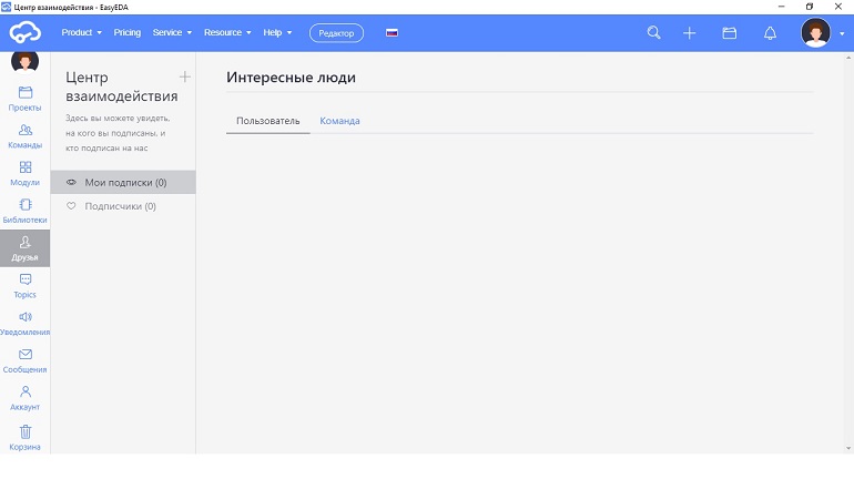
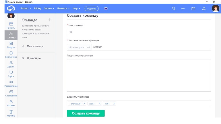
Еще одной интересной функцией центра пользователя является создание команды, например из своих подписчиков, друзей, коллег по работе. Все участники команды могут работать над одним проектом в режиме реального времени.
Создание и настройка проекта
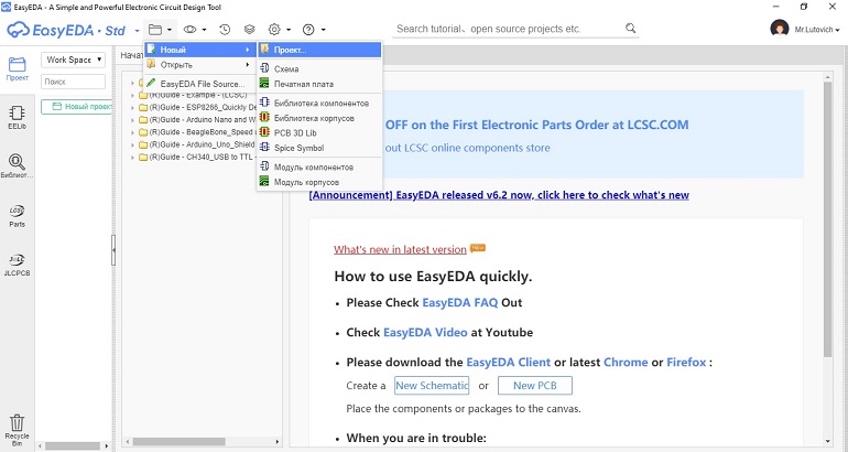
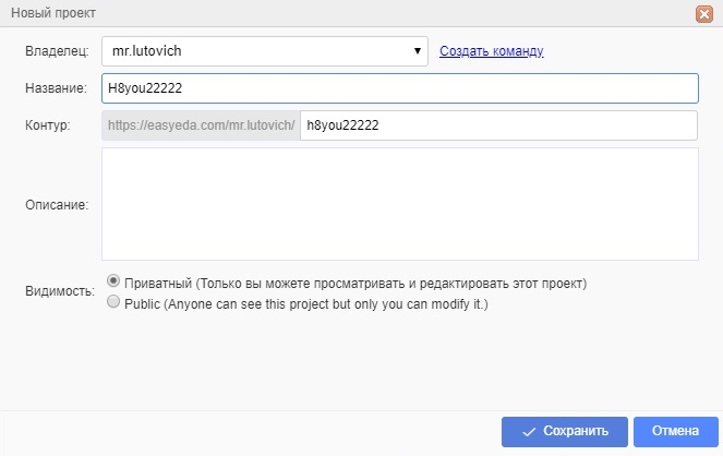
После процедуры регистрации и ознакомления с центром пользователя можно начинать работу! Для создания проекта кликаем Документ→Новый→Проект, как показано на рисунке ниже:
В модальном окне вводим название проекта (оно должно быть указано на латинице размером не менее 8 символов), описание (необязательно), выбираем параметр видимости проекта и сохраняем. Другие пользователи сервиса могут видеть ваш публичный проект. Вы можете скопировать и модифицировать проект без внесения изменений в рабочую копию.
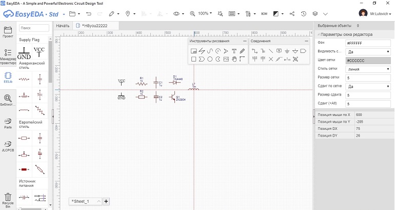
После сохранения нового проекта, открывается рабочее поле с рамкой для чертежа схемы (окно редактора). Вместе с окном редактора появляются 2 меню, первое с выпадающим списком — Инструменты рисования и Соединения, второе — боковое меню для задания параметров данного окна.
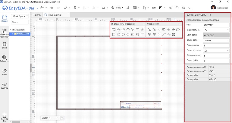
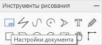
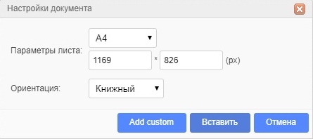
Для своих проектов я изменяю только формат листа (в зависимости от размера схемы), а также его ориентацию с помощью Инструментов рисования. Они доступны во вкладке Настройки документа в выпадающем меню. Параметры окна редактора я оставляю без изменений.
Работа с редактором схем
Для размещения компонентов схемы электрической используются вкладки левого бокового меню. Вкладка EElib в основном используется для быстрого размещения простейших компонентов, например, резистор, транзистор, конденсатор, диод.
Достаточно кликнуть курсором на нужный элемент и перетащить его на рабочее поле. И все же данную вкладку вы будете использовать редко, так как даже обычный резистор имеет различные исполнения (корпус, размер и т.п.).
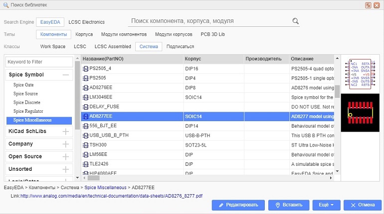
Во вкладке Поиск библиотек хранится более миллиона свежих библиотек с электронными компонентами. Все они доступны абсолютно любому пользователю сервиса. Также для удобства, вы можете создать свою библиотеку из уже существующих, часто необходимых вам компонентов и редактировать их на свое усмотрение.
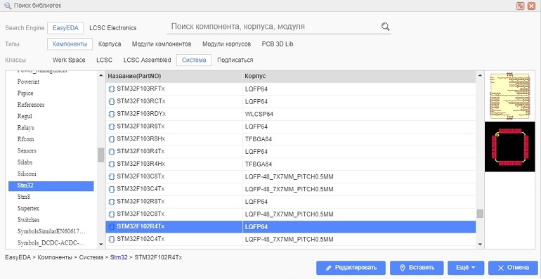
Находим необходимый компонент и жмем вставить.

Перемещение по рабочему полю осуществляется с помощью зажатого колесика мышки, а при его вращении активируется зум.
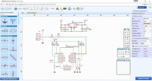
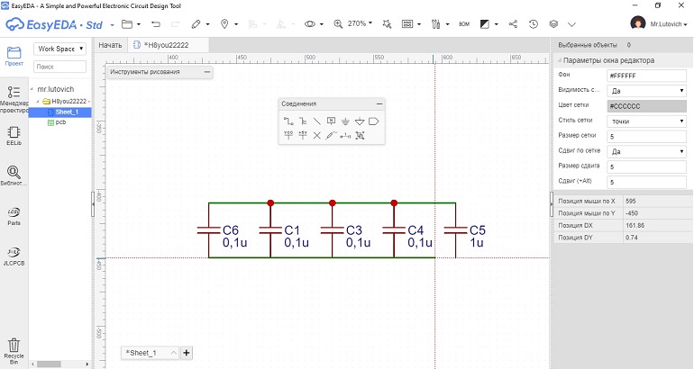
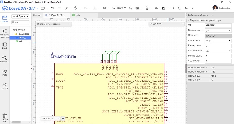
Для создания электрических связей между компонентами используется меню с выпадающим списком — Соединения. В основном элементы схемы соединяются с помощью провода, я сделал обвязку по питанию для микроконтроллера STM32F102R4Tx.
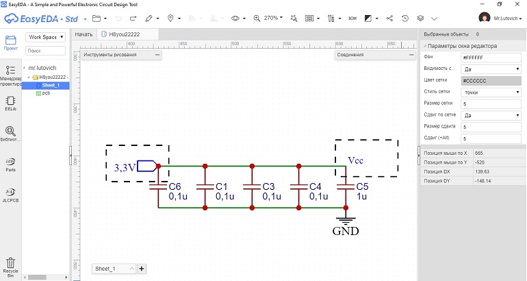
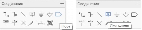
На рисунке пунктиром выделены: порт 3,3V и имя шины Vcc, которые также находятся в меню Соединения. К примеру, порты и присвоение имени шине используются для того, чтобы не тянуть провод через все рабочее поле и не загромождать схему.
Далее подключим выводы питания микроконтроллера к обвязке. Будем использовать шину и ветку шины для соединения контактов питания (веткам шины также нужно присвоить имена).
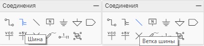
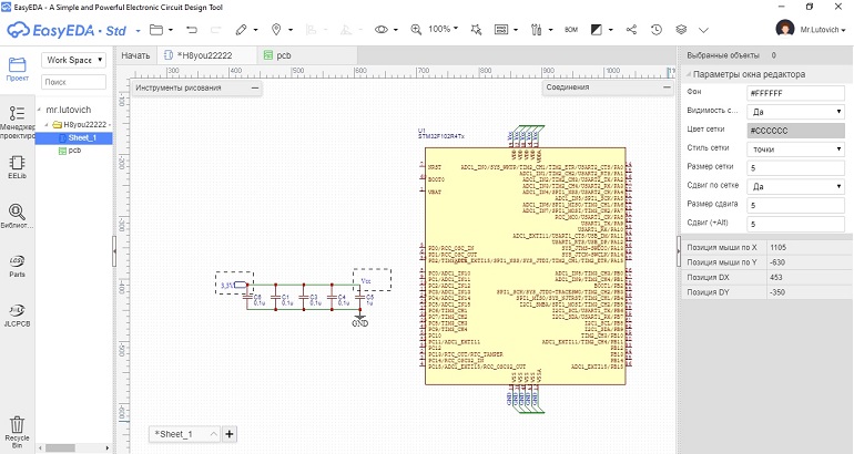
Шина, как правило, используется в местах, где локально расположено много проводов, как например в случае с выводами питания микроконтроллера. Немного забегая вперед, при генерации Gerber-файлов, сервис предложит пройти тест правил проектирования (DRC). Другими словами это тест целостности электрических соединений на схеме.
При проектировании схем на основе микроконтроллеров часто получается так, что не все его выводы используются. При прохождении DRC-теста сервис сообщит, что у нас есть неподключенные выводы и запретит создание Gerber. Неподключенные выводы или нарушения связей можно увидеть в менеджере проектирования в левом боковом меню.
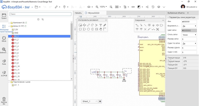
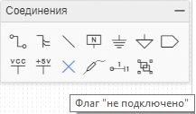
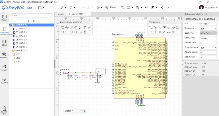
Для того, чтобы избежать неприятностей, неиспользованные выводы отметим флагом «не подключено».
На рисунке ниже результаты отметки выводов флагом «не подключено» (ошибки в менеджере проектирования отсутствуют).
Еще хотелось бы отметить, что каждый из инструментов меню Соединения активируется горячей клавишей. Например нажав W — вы сможете провести провод, а с помощью клавиши B — шину. Комбинациями Ctrl+Q и Ctrl+G вызываются флаг Vcc и флаг GND, соответственно.
Моделирование схемы электрической принципиальной
Для переключения системы в режим симуляции необходимо в левом верхнем углу изменить Std на Sim (рядом с иконкой EasyEDA). Данное переключение доступно только когда не ведется работа над каким-либо проектом и все закрыто.
Открыв вкладку EElib на левом боковом меню можно увидеть, что в режиме симуляции появились дополнительные инструменты: мультиметр, оссциллограф и генератор сигналов.
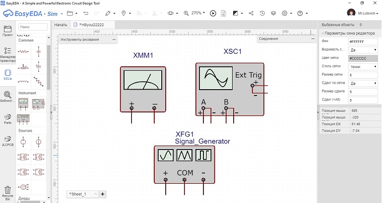
Также в EasyEDA реализована возможность симулирования на основе NgSpice. В библиотеках сервиса можно найти компоненты со spice-моделями.
Работа с редактором печатной платы
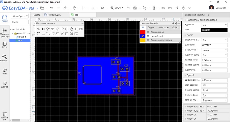
Когда электрическая схема готова и вы уверены, что она исправна, можно переходить к проектированию печатной платы. Для перехода к редактору и созданию pcb в верхнем меню во вкладке Конвертировать жмем Конвертировать в печатную плату.
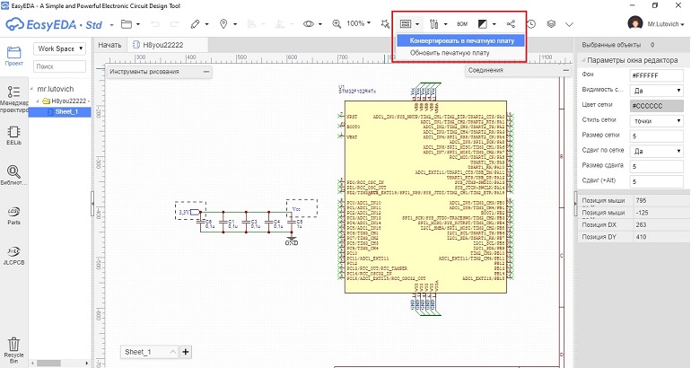
Теперь мы автоматически перемещаемся в редактор печатной платы.
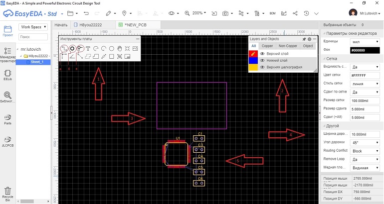
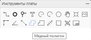
Здесь:
- Меню Инструменты платы. В этом меню есть все необходимое для рисования топологии печатной, например:
- а) Дорожка;
- б) Полигон (монтажное отверстие);
- в) Переходное отверстие;
- Меню Layers and Objects, предназначенное для работы со слоями печатной платы и составляющими ее объектами;
- Рамка ограничивающая размер печатной платы Board Outline;
- Правое боковое меню для изменения параметров окна редактора;
- Не скомпонованные посадочные места элементов печатной платы.
Сервис EasyEDA не имеет «автокомпоновщика», поэтому компонуем элементы на печатной плате вручную.
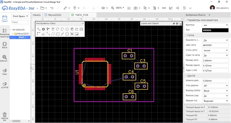
Трассировку печатной платы можно сделать как в автоматическом, так и в ручном режиме.
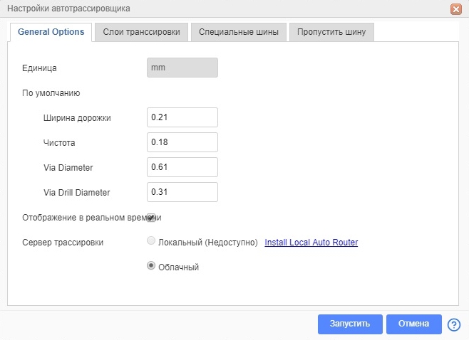
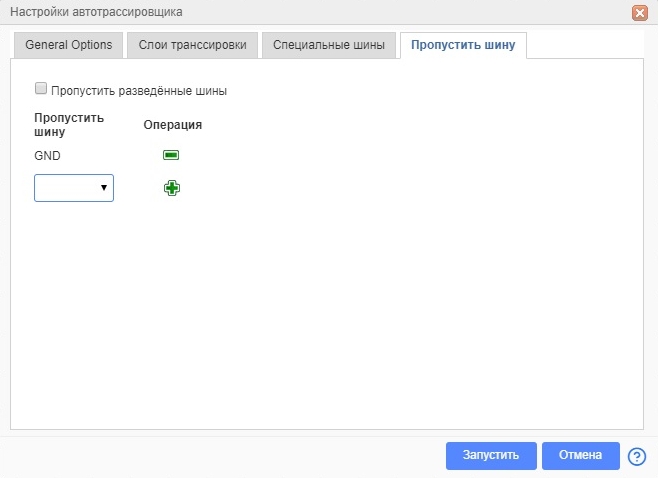
Для автотрассировки в верхнем меню редактора во вкладке Разводка нужно вызвать Автотрассировщик, предварительно изменив единицы измерения на мм (в правом боковом меню).
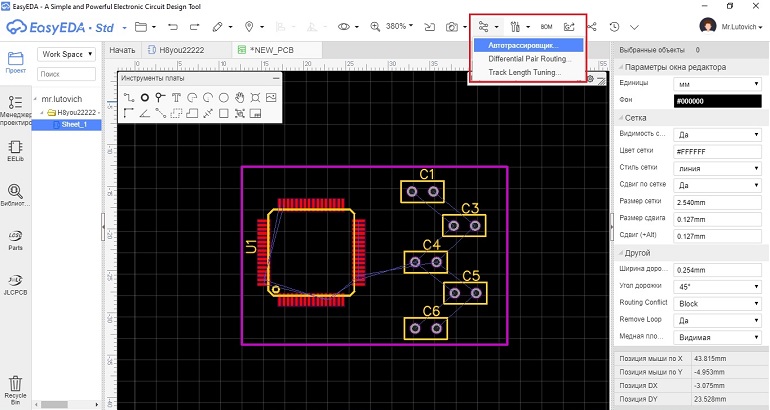
В модальном окне устанавливаем необходимые параметры трассировки и жмем запустить, пример показан на рисунке ниже:
Результат работы автотрассировщика:
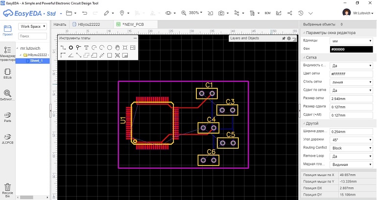
При установке параметров автотрассировщика, я отменил трассировку шины земли (GND), чтобы выполнить ее в качестве медного полигона по всему периметру печатной платы. Для этого в меню Инструменты платы выбираем Медный полигон.
Далее задаем границы медного полигона:
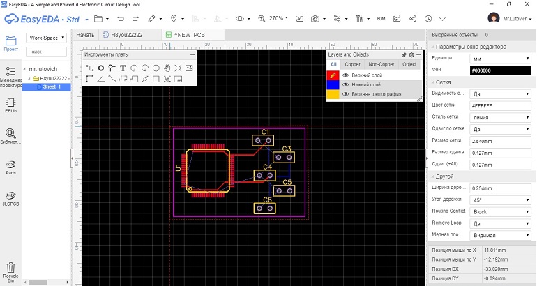
Жмем правую кнопку мыши и повторяем полигон для нижнего слоя металлизации. В итоге, мы имеем готовый проект печатной платы. Также вы можете посмотреть один из моих простеньких проектов в качестве примера.
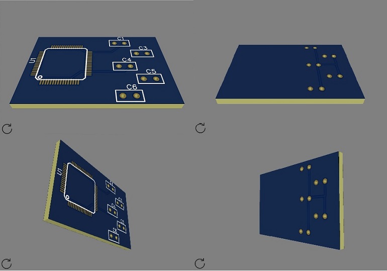
Дополнительно из редактора мы можем посмотреть, как плата будет выглядеть в 3D. Для этого в верхнем меню редактора во вкладке Предпросмотр жмем 3D View.

После загрузки мы получим 3D-модель печатной платы.
Создание Gerber и изготовление печатной платы
Когда проект печатной платы готов сразу закрадывается мысль о его изготовлении. Методы изготовления ПП в домашних условиях трудоемки и качество таких плат оставляет желать лучшего.
С помощью инструментов EasyEDA можно создать, так называемые Gerber-файлы, которые содержат в себе описание проекта печатной платы, необходимое для создания фотошаблона на спецоборудовании. Генерация Gerber не составит большого труда, для этого в верхнем меню редактора печатных плат, во вкладке Документ жмем Создать Gerber.
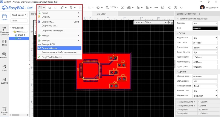
На следующем этапе сервис предложит пройти проверку правил проектирования (DRC). После прохождения теста откроется окно из которого можно:
- создать Gerber;
- заказать изготовление печатной платы на JLCPCB.
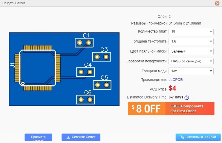
Полученный архив с файлами в формате Gerber можно отправить на предприятие по производству печатных плат для их изготовления. Если у вас нет времени на поиски изготовителя печатных плат, воспользуйтесь интеграцией EasyEDA с крупнейшим предприятием по прототипированию печатных плат в Китае, под названием JLCPCB. Читайте, как заказать на JLCPCB по ссылке.
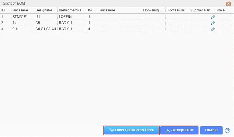
Экспорт в BOM
BOM (bill of materials) — представляет собой список компонентов, входящих в готовую плату (своеобразная спецификация), с описанием достаточным для заказа элементной базы в интернет-магазинах.
Создание BOM осуществляется по нажатию Экспорт BOM в верхнем меню редактора, во вкладке Документ.
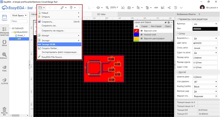
В появившемся окне выбираем: подтвердить экспорт или сразу сделать заказ компонентов у ведущего дистрибьютора электронных компонентов в Китае — LCSC.
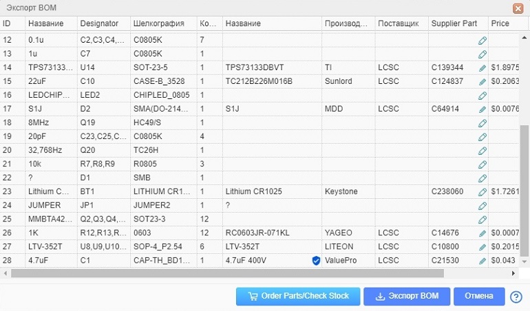
Ниже показан приличный список BOM одного из моих проектов.
Заключение
По итогам работы с EasyEDA впечатления от сервиса остались только положительные и критических недостатков, которые могли бы оттолкнуть меня от работы с ним я не нашел. Прочитав данное руководство, любой желающий или хоть немного увлекающийся электроникой сможет воплотить в реальность проект своего электронного устройства.
Creating The Schematic
During this tutorial we will create a simple Schematic design to guide you in using EasyEDA Schematic capture.

Canvas Settings
You can find the canvas Properties setting by clicking on any the blank space in the canvas.
![]()
As described earlier, background and grid colours and the style, size, visibility and snap attributes of the grid can all be configured.
The canvas area can be set directly by the Width and Height or by using the available preset frame sizes.
Grid
Visible Grid : Yes or No
Grid Color: Any valid colour
Grid Style: Line or Dot
Grid Size: To ensure proper alignment of all EasyEDA parts, it is advisable to set in 10, 20, 100.
Grid (and background) colour can be set directly by entering the hexadecimal value of the colour you want or by clicking on a colour in the palette that opens when you click on the colour value box:

Snap
Snap: Yes or No. The default hotkey is G. Pressing this key toggles switching snap to grid on and off.
Snap Size: To ensure proper alignment of all EasyEDA parts, it is advisable to set in 10, 20, 100 but any valid number can work, such as 0.1, 1, 5.
It is strongly recommended that you keep Snap = Yes all the time. Once items are placed off-grid it can be very difficult to reset them back onto the grid. Off-grid placement can result in wires looking as though they are joined when in fact they are not and so causing netlisting errors that can be hard to track down.
If you need to draw detailed parts of new symbols or footprints that need to go between grid points, try to reduce the grid spacing to draw these elements and then reset the grid back to your chosen default value as soon as you have completed that part of the drawing. Setting Snap=No should only really be used as a last resort.
ALT Sanp: Snap size when pressing the ALT key.
Wiring Tools
If you have hidden your tools , you can open them from here:
Top toolbar Config Gear Icon > Toolbars > …
![]()
Note: All of the commands in Wiring Tools are electronics related. Don’t use a wire when you just need to draw a line, shape or an arrow: use Drawing Tools instead.

Wire
There are three ways to enter the wire mode in EasyEDA.
- Click the Wire button from the Wiring Tools palette.
- Press the
Whotkey. - Click on the end of a component pin (where the grey pin dot appears if you select the component):

EasyEDA automatically enters Wire mode.
Here is a screenshot of the Astable Multivibrator LED project schematic after wiring:

Moving Components And Wires:
If you place a component, such as a resistor, on top of a wire then the wire breaks and reconnects to the ends of the component.
When moving selected components using the mouse, they will drag attached wires with them (“rubber band”) to some extent but please be aware that the rubber banding feature has some limitations. When moving selected components most wire will move vertically and horizontally. Using the arrow keys will not rubber band. Selected wires do not rubber band.

A selected wire can be moved directly by clicking on it using the mouse or by the arrow keys. If a wire is selected by clicking on it using the mouse then green grab handles will appear at the ends and vertices.
Auto adjust connection
If you put a resistor or capacitor on a wire, the wire will auto connect the pins as below:

When you want to wiring a series of resistors which are in a row, you can just wire through them, and then you will find they all be connected.

Bus
When you design a professional schematic, perhaps it will use a lot of wires. If you’re wiring one by one, much time would be wasted, and then you need to use Bus.

Bus Entry
If you decide to wire with Bus , the Bus Entry must connect to Bus and other nets with wires. such as in the above image.
Net Label
NetLabel and NetFlag
NetLabel can be used to give your wires names to help you find them and identify any misconnections. You can find the NetLabel from the Wiring Tools palette or by using the N hotkey. When selecting the netlabel, you will find its attributes in the right hand Properties panel:

You can change its name and colour. If you only want to change its name, it may be easier to just double click the netlabel.
Net Flag
NetFlag is the same as NetLabel, you can find the NetFlag from the Wiring Tools palette or using the Ctrl+G hotkeys for GND or Ctrl+Q for VCC. You can also change its name, for example from VCC to VDD:

The screenshot below is after adding NetLabels
- indicated by the little egg marks
-and a GND NetFlag
This schematic is almost finished.

Wiring Tools palette provides NetFlag: Digital GND, Analog GND, VCC and +5V for your convenience.
Net Port
When you don’t want to route too many wires, how about trying Net Port :

It will make your schematic look more clean, and you just need to set each Net Port a net name.

No Connect Flag
You can find the NO Connect Flag via wiring tool,
 ,
,
In the below schematic, if you don’t add a NO Connect Flag, there is an error flag in the nets collection of the design manager.

After adding a NO Connect Flag, the error disappears.

Note: NO Connect Flag only works on the symbol’s pin directly.
Voltage Probe

EasyEDA provides a simulation feature for the schematic. After the simulation is running, you will see the waveform where you placed the voltage probes in the circuit.

For more detail about the simulation, please check the Simulation section.
Pin
When you create a new symbol in schematic and schematic lib, you must use Pin to create pins for the new symbol, otherwise your symbol can’t be wired with wires.

For more information please refer to the Schematic Lib: Pin section.
Group/Ungroup
On the Wiring Tools palette there is the Group/Ungroup Symbol… button.

Just like the Symbol Wizard, this tool is also for you to quickly create schematic library symbols.
Using the Symbol Wizard you can only create generic symbols but how can you quickly and easily create symbols like these?

Here’s how.
EasyEDA allows you to do something that very few other EAD tools support.
Using the P Hotkey, you are allowed to add a PIN directly onto the Schematic canvas. So you can add 8 Pins, draw a rectangle from the Drawing Tools palette and add 555 as text to form a symbol for the NE555 like the one shown below:

Now comes the clever bit.
Up to this point you have a collection of separate pins, a drawn rectangle and some text that are all separate items with no particular association with each other.
So now select all of the items and click the Group/Ungroup Symbol… button. A dialog will be opened:

After you click OK, all those separate elements will be grouped together to form your new symbol directly in the schematic.
Using the group function, you can create any symbol in the schematic, easily and quickly.
How cool is that?
So what does Ungroup do? Try selecting a symbol and then click the Group/ungroup command to see what happens!
Note: The pin numbers and names cannot be moved independently of the pin.
If it’s still difficult to understand, don’t worry, you can see the process in the dynamic image below:

Drawing Tools
Sheet Setting
It is now possible to add design notes to the frame and the frame selection, for example A4, which can assist in aligning and improve the look of printed schematics and PCB designs.
Click the frame button like in the image below, Or via: Super Menu > Miscellaneous > Sheet Setting

As illustrated in the image below:

And you can edit the blue text when you’ve selected the text attributes or double clicked it.
The bottom right zone can be selected and dragged or the frame can be dragged and deleted.
When you’ve selected the bottom right zone, you can edit the sheet attributes:

Line
In the Schematic editor, you can draw a line with any direction. You can change its attribute as in the image below:

Bezier
With this tool, you can draw a pretty cool pattern.

Arc
You can draw the arc of any shape.

Arrow Head
You can add arrow head to marking text or important part.
![]()
Text
Text attributes provide many parameters for setting:
- Text: You can change text in inner box or double click the text. For every new text, the default text is
Text.
—Color: Defines text color.
—Font-family: It provides 12 fonts for choosing.
—Font-Size: Defines Text size.
—Font-weight: Defines Text weight.
—Font-Style: It contains (auto), normal, italic.
—Text-anchor: It contains (auto), start, middle, end, inherit.
—Baseline: It contains (auto), use-script, no-change, reset-size … and so on.
—Text type: types include comment and spice.
The editor will remember your last text parameters.

Image
When you select Image from the Drawing Tools palette, an image place holder will be inserted into the canvas:

Select the place holder, so you can see the image’s attributes in the right hand Properties panel:

Set the URL of your image. For example, setting the URL to:
http://upload.wikimedia.org/wikipedia/commons/thumb/c/c7/555_Pinout.svg/220px-555_Pinout.svg.png
will make your image look like this:

Please note: at present, EasyEDA cannot host images, so you need to upload your images to an image sharing site such as http://www.imgur.com.
Drag
If you want to move some kind of parts and wires, you can use drag.
Or you can select the parts and wires area first and move them.

Canvas Origin
Canvas origin default is set at left top corner of the schematic sheet, but you can set it where you want via Canvas Origin.
For another way to set canvas origin, you can try Super Menu > Miscellaneous > Canvas Origin.

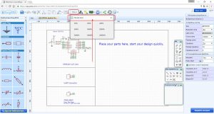
Search symbols
On the left hand Navigation panel you will find «EElib» and «Parts» ,
- EELibs contains ready made symbols for a wide range of components and which can be simulated.

Many of these components have optional US and EU style symbols, we split them, so you can select those you like. Click on the drop down list or right click to popup the context menu, it contains many packages or parameters. EasyEDA will remember your choices for the next time.
Don’t forget to use Filter to locate a component fast. For example, you just need to type res to find all of resistors:

- Parts, or press the hotkey combination
Shift+F.
then you will see a dialog as shown in the image below.
Simply type your part number or symbol’s name to Search.

and then click the “Table of contents” to open the categories list to choose your components.
From there you can scroll up and down to browse parts from each category.
Suppose you wanted the find the MAX232 (which converts signals from an RS-232 serial port to signals suitable for use in TTL compatible digital logic circuits). Simply type Max232 into the Search box and press Enter:
When you hover the mouse over the picture of the Schematic symbol or PCB footprint, you will find a toolbar with «Edit”, “Place”, “More” buttons.
LCSC Assembly Components
We add an LCSC Assembly Components option of the Parts, It’s easy to choose which component can be assembled by LCSC. Yes, We provide the assembly service.

Place:
For parts you use infrequently, you don’t need to Favorite them; just Place it into your canvas directly.
Note:
-
EasyEDA supports multi-documents so please make sure that you are placing the part into the right (active) document. The active document is the one with the highlighted tab.
-
You can’t place a Schematic symbol into a PCB file, or a PCB Footprint into a schematic.
Edit:
If you want to create your own version of a symbol or footprint then you can open an existing part from the library to use as a template, edit it and then save it to your local My Parts library in Parts of the Navigation Panel.
More:
We can’t promise that every component in the library is free of errors so please check all symbols and footprints carefully before you commit to a PCB order.
If you do find a mistake in a component, please let us know(mail to support@easyeda.com) so that we can fix it.
Components with sub parts (multi-device packages).
When you find a component with sub-parts, you can’t Place or Edit it, but you can Favorite and Clone it as your own part, which you can then edit.

Find Components In The Schematic
Finding individual components in a dense schematic can be very time consuming. EasyEDA has an easy way to find and jump to components:
Super Menu > Miscellaneous > Find Component…
(or Ctrl+F)

Note: You have to click OK in this dialog or use the Enter key.
This feature will find, highlight and center in the window, parts by their Prefix (or reference designator). However, it cannot be used to find net names or other text in a schematic.
This is where the Design Manager comes in.
Left Navigation Panel > Design, or use hotkey ctrl+D.
The Schematic Design Manager is a very powerful tool for finding components, nets and pins.
Clicking on a Component item highlights the component and pans it to the center of the window.

Clicking on a Part pins item brings up a temporary pointer:

Placing Components
Find the component which you plan to place to your schematic, then move your mouse to the canvas and left click. If you want to add more, just left click again. To end the current sequence of placements, right click once or press ESC.
Don’t try to Drag and Drop a component to the canvas: EasyEDA team thinks that Click-Click to place components will be easier to use than a Click-Drag mode.

Rotating the Prefix and Value (Name) of components
The default Prefix and Value (or name) of EasyEDA components are horizontal. To change them to vertical like this…

…Left click the prefix or value and when it is highlighted in red color, then press the rotation hotkey Space and you’re done.
Adjusting Components
About adjusting components you can:
- Move components with your mouse
- Move components with the arrow keys.
- Find components with the Design Manager via the
CTRL+Dhotkey: select the component in the Design Manager to pan it to the centre of the canvas and then move it with your mouse. - Align the components:

Cross Probe

This tool is used to cross probe from chosen objects on the current schematic to its corresponding counterparts in the PCB, or from PCB Footprints to corresponding counterparts in the schematic.
Note:
- You don’t need to open PCB first before using cross probe in the schematic. Editor will open the PCB automatically.
And don’t forget to use the hotkeySHIFT+X.

Cross Probe And Place
If your schematic have a lot of components, it will be difficult to layout the PCB , so EasyEDA provides a powerful function «Cross Probe And Place».
Topbar > Tools > Cross Probe And Place
Cross Probe And Place will make the footprints’ location match the schematic’s parts’ location as much as it possibly can.

How to use:
- Converting Schematic to PCB first, and save at current project.
- Select the components area by mouse in the schematic, and then click the «Cross Probe And Place», hotkey «CTRL + SHIFT + X».
- The editor will switch to the PCB, and choose the footprints as you selected for waiting for placing.
- Right click to place, and the mouse will keep the drag status, its easy for adjusting the footprints’ location.

Notice:
- You don’t need to open PCB first before using this function in the schematic. Editor will open the PCB automatically.
- If your project has many PCBs, and didn’t open anyone yet, the editor will open the first one automatically; If you already open a PCB, and this function will be valid for this PCB.
Design Manager
With large schematics it can be hard to find the components quickly. Sometimes, you may make a mistake such as wiring to a wrong component pin. So you need a tool to help you out. Design Manager is just the tool.
Just press the CTRL+D hotkey to open the Design Manager.
or click it via on the left navigation panel:

- Filter: You can find your components or net name easily: for example, if you want to find all capacitances, you just need to type
C; - Components: Lists all the components in this schematic. Clicking on a Component item highlights that component and pans it to the center of the window.
- Nets: Lists all the nets in this schematic. A net must connect at least two Pins, or the net name will be marked as a red error.
- Net Pins/Parts Pins: Lists all the pins of the selected net name or components.
If you click the Q1 Pin 1:VCC, EasyEDA will show you where it is with a temporary marker from the top left of the canvas:

Footprint Manager
Want to batch modify components? Can’t identify the corresponding relationship between component pins and footprint pins? Don’t worry, EasyEDA can do this.
There are two ways to open the footprint manager:
-
Click top toolbar Tools icon:
-
Click the package input box of custom attributes when you’ve selected a component:


1. Footprint manager will check your parts package correct or not automatically. If the part without the package or this package doesn’t exist in EasyEDA Libraries, or if the part’s Pins doesn’t correspond the package’s Pads correctly, the footprint manager will show the red alert.
For example, If your part U1 has 2 pins, pin number are 1 and 2, pin name is A and B, but you assigned a footprint has 2 pads, pad number are A and B, but the part’s pin number doesn’t match the pad number, so the the footprint manager will alert red, in order to solve this:
- method 1: change part’s pin number as A and B.
- method 2: change package’s pad number as 1 and 2.
- method 3: find an other package and update.
2. In the preview area, you can zoom in, zoom out and pan with mouse.

Update Package
If you want to change the Package, for example, select a component such as Q1, from TO-92 TO TO220, you just need to click in the package input box. EasyEDA will popup the footprint manager dialog. You can follow the instructions.
- Type TO220 into the search box and search,
- Select the TO220 package,
- Verify it in the preview box,
- then press the Update button.
After that you will find you have changed the package to TO220.
Note: To ensure that you use a package type that is already in the EasyEDA libraries, it is recommended that you use this technique to change component packages rather than just typing a package type directly into the package text box.

Batch Update/Modify Packages
If you want to batch modify components’ packages, in the footprint manager dialog you can press CTRL and select all components you want. If your schematic has many components, you should filter them first with package name. Such as in the below .gif which will show you how to batch modify resistors’ packages from AXIAL-0.3 to 0603.
If you want to use your own packages, you can select My Parts on Pattern Libraries area.

Modify Pin Map Information
And you can modify component’s pin map information in here.
Annotate
After creating a schematic, it is quite likely that you have component Prefixes (reference designators) that are in no particular order on the canvas. You may also have duplicates. You can automatically renumber all the components using the Annotate function.
Super menu > Miscellaneous > Annotate

Various Annotate possibilities are available:
- Active Schematic only: applies annotation actions to the current schematic only.
- All Opened Schematics: applies annotation actions to all Schematics that are open in EasyEDA.
Note: This option applies even if the opened schematics are from different Projects! If the project that you want to annotate has more than one schematic, you should open all of them and close any schematics that are open from other Projects.
- Re-annotate all: resets all existing annotation and then annotates all components again from scratch;
- Keep existing annotation: annotates new components only (i.e. those whose reference designator finishes with ? like R? or U?).
- Direction: Rows annotates across the schematic in a raster pattern from top left to bottom right; Cols annotates down the schematic in a raster pattern from top left to bottom right.
- Annotate: applies the selected annotation actions.
Note: Annotation cannot be undone! if you do not accept the result: close all of the affected schematics without saving. If you do accept the result: make sure you save all of the affected schematics.
- Reset: if you want to reset all the reference designators to end with ‘?’, just click the Reset button. After that, R1 will be R?, U1 will be U? etc.
Note: Reset does not reset annotation back to where it was before pressing the Annotate button.
Symbol Wizard
How many times have you hit a schematic capture roadblock because you couldn’t find a component symbol?
Well, in EasyEDA that would be never because the Symbol Wizard provides a quick and easy way to create a general schematic library symbol.
The Symbol Wizard… command can be found in the top toolbar.
Or Super Menu > Miscellaneous > Schematic Library Wizard in a new schematic lib document.

Using the NE555 timer as an example: this device is available in a DIP8 package so select DIP. Then enter the NE555 pin names into the Pin Names text box separated by new line or space, Then press OK. Abracadabra! As if by magic, you will find a perfectly formed dual in line 8 pin symbol for the NE555 attached to your mouse cursor, ready to be placed! You just need a few seconds to build a NE555 symbol, quickly and easily.

The EasyEDA Schematic Symbol Wizard allows you to create DIP, QPF or SIP styles symbols. If you are designing Arduino Shields then you will need lots of SIP symbol, so you can create a SIP symbol like the one shown below in a few seconds.

If you are not too worried that the symbols may not look quite the way people might expect and that they may not look anything like the Package type you enter, then of course you can use the wizard to create symbols for any component:

Multi-part Components
The number of pins on some components can be quite large. That’s why it’s easier to divide such a component into several parts or functional blocks. As a simple example, there are six gates in the 74HC04 Hex Inverter component. To avoid clutter in the schematic, GND and VCC pins of such components are usually served by a separate part of the component. This is really convenient as it doesn’t interfere the working process with logical parts. The NetLabel names of VCC and GND Pin are usually hidden.
When placing the 74HC04 on a schematic, it will look like the screenshot below.
Note: The component Prefix will be in form of: U?.1, U?.2 etc.

Component Attributes
After selecting a component, you can find the component’s attributes in the right hand Properties panel.

**1.**Part Attributes: You can change the Prefix and Name here,And make them visible or invisible.
If you want edit this component, you can click Edit Symbol.

**2.**Custom Attributes: You can change component’s supplier, mounted or not, change package, and add new parameter.
Define BOM Parameters
After selected a schematic symbol, you can add a parameter, and you can mark it as In BOM, when you export a BOM file, you can find this parameter in CSV file.

Pinmap Modify Symbol Information
When you select a component, for opening the Modify symbol information dialog, you can do:
1.****Super menu > Miscellaneous > Edit Symbol…;
**2.**Or press the I hotkey;
**3.**Or click the Edit Symbol on the Parts Attributes on the left panel.
Using this dialog you can edit the pin names and numbers, for example, to suit a different package or device variant. You can also enter a Spice Prefix and swap the spice Pin order to make your symbol usable in simulation.
More detailed description of PCB and Spice Prefixes and pin numbers at next section.
Prefixes And Pin Numbers
Device and subcircuit (or hierarchical block) symbols created for use in schematics that are intended to be run as spice simulations, in addition to having a PCB Prefix that is used for the reference designator in the schematic, also have a Spice Prefix. They also have two sets of pin numbers: PCB pins and Spice pins.
PCB And Spice Prefix
The rules on the assignment of the PCB Prefix or reference designator of a schematic symbol are somewhat dependent on the EDA tool and on the user’s preferences. Depending on how a device is graphically represented by its schematic symbol it may have a different PCB Prefix or** reference designator**. For example, a single discrete MOSFET device may have a PCB Prefix of Q, M or perhaps TR, whereas if it is part of a monolithic multiple transistor array it may have a PCB Prefix of U or IC.
The rules on the assignment of the Spice Prefix of a schematic symbol are strict. This is because the Spice Prefix is used to tell the simulator which circuit element the symbol represents and therefore which simulation model it is to use.
Simulation models for most of the spice circuit elements are in the form of a single-line .model statement however some of them may be in the form of a multi-line .subckt subcircuit definition. For example, some MOSFETs may be described by a .model statement in which case their Spice Prefix is M but many MOSFETs are described by a .subckt and so their Spice Prefix is X.
Therefore, irrespective of the PCB Prefix chosen for a schematic symbol, the Spice Prefix for a schematic symbol representing a given circuit element must match the type of model required to simulate that instance of that circuit element in your schematic.
A list of Spice Prefixes and their associated circuit elements is given in the table below.

For more information on circuit elements in Ngspice, please refer to:
http://ngspice.sourceforge.net/docs/ngspice-manual.pdf#subsection.2.1.2
PCB and Spice pin numbers
The two sets of pin numbers are:
-
**PCB pin number: **these are the numbers for the real, physical device pins in its package. They are required so that the pins of a device symbol in a schematic can be mapped onto the physical pins of a PCB footprint. In other words, so that the connections shown in the schematic, end up connected properly by copper on the PCB.
-
**Spice pin number or pin order: ** these are the numbers that map the pins on the symbol to their respective functions in the spice model or subcircuit.
Prefix Start
Every NEW schematic file has a Prefix Start custom parameter, some users would like use multi-sheet designs, but they hate every prefix start by 1, they hope one schematic start by 1, next start by 100, 200, 300. So you can use this solution.

Prefix Conflict Error
Sometimes, when you convert a project to PCB, open the Design manager or run a simulation, you will get a Prefix Conflict error message.

In this schematic, you will find two components with the R4 reference designator, so you just need to change one to Rx where x is a unique number in that schematic.
It may be tempting to backup a schematic into the same project as the original, however, if an attempt is then made to do Convert Project to PCB, you will get the Prefix Conflict error for every component.

In the above image, you can find the two identical copies of the same schematic, which when you Convert Project to PCB, EasyEDA will try to merge into a single schematic, so every item will have 2 copies.
To fix this, you just need to create a backup project and remove or better still save backup copies of your schematics to that project.
Multi-NetLabels in One Wire
EasyEDA support mutil-netlabel in one wire now.
When you convert the schematic to the PCB, the editor will choose the first netlabel you placed as the net name for this wire, as below NETLABEL1.

As above image, when you click anyone netlabel’s name in the design manager, the wire will be highlighted.
Notice:
- If wire 1 has 3 netlabels A B and C, and wire 2 has netlabel A, then wire 1 and wire 2 are the same net.
Converting Schematics To PCB
Before using «Convert to PCB», «Update PCB» in Schematic and «Import Changes» in PCB, please read Essential Check section.
Most of the time, schematics are created with the aim of producing a PCB. So how do you convert your schematic to a PCB in EasyEDA? You just need to to click the PCB icon on the toolbar with the title Convert project to PCB.
Note: Before converting, you need to use the Design Manager and Footprint Manager to check all the components, nets(connection) and packages/footprints to ensure no errors exist.

PCB Libs search order
To find PCB footprints to match the package type attributes of your Schematic symbols, EasyEDA will search the available PCB libraries.
EasyEDA will search your own PCB Libs from the My Parts section first. If it doesn’t find a matching footprint there then it will search in the System PCB Libs.
So, for example, if your symbol calls up a “TO220” package, you have a TO220 package in your My Parts section and there is a “TO220” package in the system PCB Libs, then EasyEDA will use the “TO220” package in your My Parts and ignore the system PCB Lib.
Verify Packages and Build PCB
After clicking the Convert project to PCB button, if the project has errors the following dialog will open:

The row in red indicates that EasyEDA can’t find a PCB footprint matching the Package that the schematic symbol is calling for.
This could be because you have made an error entering the package attribute in the symbol’s Properties or maybe you haven’t yet created a PCB footprint for the package that your symbol is calling for.
In this case the package should have been TO-92(TO-92-3) but instead it is empty. To correct it you can click on the row and change it to TO-92(TO-92-3).
After making any necessary corrections, click the Convert project to PCB button and EasyEDA will automatically load all the package PCB footprints into the PCB editor as shown in the image below.

This shows the footprints placed in arbitrary positions with the connections between them shown as blue Rat lines.
Update PCB
Converting a schematic to PCB can be done using the Convert Project to PCB... , but if you do modifications to the schematic, by using the Update PCB button you can immediately be passed forward to update the selected PCB without having the PCB editor window already open or without creating a new PCB file.

Hierarchy
EasyEDA does not support true hierarchical designs but it does support multi-sheet designs. You can put several schematics in one project with connections between made by netlabels. All nets in EasyEDA are global so if you create a netlabel DATA0 in schematic A and then create a netlabel DATA0 in schematic B, when Schematic A and schematic B are in the same project, they will be connected.

Multi-sheet designs(equivalent to a circuit spread over several pieces of
paper), all schematics under the same project will be merged into one when be converted to PCB connecting in netlabe, netflag.

Note:
Please make all of the prefixes unique, if the Schematic A has a R1, and the Schematic B has a R1, then you will get a Prefix Conflict Error on above section.
Tip:
Every schematic’s prefix will start from 1, such as R1, C1, U1 etc.
1. you can use Annotate to fix prefix.
2. You can set the prefix start to 100, then your components will start from R100, C100.
Modules
Copying codes is an easy job for coders, now copying and reusing a schematic or PCB is easy.
Take a power supply unit for example, you can save this unit as a schematic module.

After saving, you can find it at the Parts > My Modules section. And you can place the whole block to your schematic.

BOM/Netlist
Export BOM
You can export the Bill of Materials (BOM) for the active schematic (Document) and PCB or for the active project (i.e. the BOM for all the sheets in the project) as shown below,click the top toolbar BOM icon:
![]()
After clicking the BOM export option, the dialog below will open.
In this dialog,you can assign LCSC part’s order code for your components.

After clicking on the assign icon,the components and packages search dialog will pop up, and you can choose which component you want to assign.

When you click «Export BOM at LCSC», we will help you to list all the components of your BOM, If you want to buy the components form LCSC, and you just need to put them to the cart and check out.


And Click the «BOM» button to download the BOM file. You can open it in any text editor or spreadsheet.

Export Netlist
EasyEDA can export the netlist for the active schematic (Document) and/or for the whole active project:
Super menu > Miscellaneous > Netlist for Document or Netlist for Project
EasyEDA can export a netlist in a variety of formats:
- Spice: this is a Spice3f5 compatible netlist generated by the simulation engine of EasyEDA, Ngspice. It is not normally used as the basis for as a PCB layout.
- KiCad: a PCB netlist in a format that can be imported straight into Pcbnew, the PCB layout tool part of the free, open source cross-platform EDA suite.
- Altium Designer: a PCB netlist in a format that can be imported straight into Altium Designer and it’s predecessor, Protel.
- Pads: a PCB netlist in a format that can be imported straight into Pads PCB layout tools.
- FreePCB: a PCB netlist in a format that can be imported straight into FreePCB, a free, open source PCB editor for Windows.

Creating The Schematic
During this tutorial we will create a simple Schematic design to guide you in using EasyEDA Schematic capture.
Canvas Settings
You can find the canvas Properties setting by clicking on any the blank space in the canvas.
![]()
As described earlier, background and grid colours and the style, size, visibility and snap attributes of the grid can all be configured.
The canvas area can be set directly by the Width and Height or by using the available preset frame sizes.
Grid
Visible Grid : Yes or No
Grid Color: Any valid colour
Grid Style: Line or Dot
Grid Size: To ensure proper alignment of all EasyEDA parts, it is advisable to set in 10, 20, 100.
Grid (and background) colour can be set directly by entering the hexadecimal value of the colour you want or by clicking on a colour in the palette that opens when you click on the colour value box:
Snap
Snap: Yes or No. The default hotkey is G. Pressing this key toggles switching snap to grid on and off.
Snap Size: To ensure proper alignment of all EasyEDA parts, it is advisable to set in 10, 20, 100 but any valid number can work, such as 0.1, 1, 5.
It is strongly recommended that you keep Snap = Yes all the time. Once items are placed off-grid it can be very difficult to reset them back onto the grid. Off-grid placement can result in wires looking as though they are joined when in fact they are not and so causing netlisting errors that can be hard to track down.
If you need to draw detailed parts of new symbols or footprints that need to go between grid points, try to reduce the grid spacing to draw these elements and then reset the grid back to your chosen default value as soon as you have completed that part of the drawing. Setting Snap=No should only really be used as a last resort.
ALT Sanp: Snap size when pressing the ALT key.
Wiring Tools
If you have hidden your tools , you can open them from here:
Top toolbar Config Gear Icon > Toolbars > …
![]()
Note: All of the commands in Wiring Tools are electronics related. Don’t use a wire when you just need to draw a line, shape or an arrow: use Drawing Tools instead.
Wire
There are three ways to enter the wire mode in EasyEDA.
- Click the Wire button from the Wiring Tools palette.
- Press the
Whotkey. - Click on the end of a component pin (where the grey pin dot appears if you select the component):
EasyEDA automatically enters Wire mode.
Here is a screenshot of the Astable Multivibrator LED project schematic after wiring:
Moving Components And Wires:
If you place a component, such as a resistor, on top of a wire then the wire breaks and reconnects to the ends of the component.
When moving selected components using the mouse, they will drag attached wires with them (“rubber band”) to some extent but please be aware that the rubber banding feature has some limitations. When moving selected components most wire will move vertically and horizontally. Using the arrow keys will not rubber band. Selected wires do not rubber band.
A selected wire can be moved directly by clicking on it using the mouse or by the arrow keys. If a wire is selected by clicking on it using the mouse then green grab handles will appear at the ends and vertices.
Auto adjust connection
If you put a resistor or capacitor on a wire, the wire will auto connect the pins as below:
When you want to wiring a series of resistors which are in a row, you can just wire through them, and then you will find they all be connected.
Bus
When you design a professional schematic, perhaps it will use a lot of wires. If you’re wiring one by one, much time would be wasted, and then you need to use Bus.
Bus Entry
If you decide to wire with Bus , the Bus Entry must connect to Bus and other nets with wires. such as in the above image.
Net Label
NetLabel and NetFlag
NetLabel can be used to give your wires names to help you find them and identify any misconnections. You can find the NetLabel from the Wiring Tools palette or by using the N hotkey. When selecting the netlabel, you will find its attributes in the right hand Properties panel:
You can change its name and colour. If you only want to change its name, it may be easier to just double click the netlabel.
Net Flag
NetFlag is the same as NetLabel, you can find the NetFlag from the Wiring Tools palette or using the Ctrl+G hotkeys for GND or Ctrl+Q for VCC. You can also change its name, for example from VCC to VDD:
The screenshot below is after adding NetLabels
- indicated by the little egg marks
-and a GND NetFlag
This schematic is almost finished.
Wiring Tools palette provides NetFlag: Digital GND, Analog GND, VCC and +5V for your convenience.
Net Port
When you don’t want to route too many wires, how about trying Net Port :
It will make your schematic look more clean, and you just need to set each Net Port a net name.
No Connect Flag
You can find the NO Connect Flag via wiring tool,
,
In the below schematic, if you don’t add a NO Connect Flag, there is an error flag in the nets collection of the design manager.
After adding a NO Connect Flag, the error disappears.
Note: NO Connect Flag only works on the symbol’s pin directly.
Voltage Probe
EasyEDA provides a simulation feature for the schematic. After the simulation is running, you will see the waveform where you placed the voltage probes in the circuit.
For more detail about the simulation, please check the Simulation section.
Pin
When you create a new symbol in schematic and schematic lib, you must use Pin to create pins for the new symbol, otherwise your symbol can’t be wired with wires.
For more information please refer to the Schematic Lib: Pin section.
Group/Ungroup
On the Wiring Tools palette there is the Group/Ungroup Symbol… button.
Just like the Symbol Wizard, this tool is also for you to quickly create schematic library symbols.
Using the Symbol Wizard you can only create generic symbols but how can you quickly and easily create symbols like these?
Here’s how.
EasyEDA allows you to do something that very few other EAD tools support.
Using the P Hotkey, you are allowed to add a PIN directly onto the Schematic canvas. So you can add 8 Pins, draw a rectangle from the Drawing Tools palette and add 555 as text to form a symbol for the NE555 like the one shown below:
Now comes the clever bit.
Up to this point you have a collection of separate pins, a drawn rectangle and some text that are all separate items with no particular association with each other.
So now select all of the items and click the Group/Ungroup Symbol… button. A dialog will be opened:
After you click OK, all those separate elements will be grouped together to form your new symbol directly in the schematic.
Using the group function, you can create any symbol in the schematic, easily and quickly.
How cool is that?
So what does Ungroup do? Try selecting a symbol and then click the Group/ungroup command to see what happens!
Note: The pin numbers and names cannot be moved independently of the pin.
If it’s still difficult to understand, don’t worry, you can see the process in the dynamic image below:
Drawing Tools
Sheet Setting
It is now possible to add design notes to the frame and the frame selection, for example A4, which can assist in aligning and improve the look of printed schematics and PCB designs.
Click the frame button like in the image below, Or via: Super Menu > Miscellaneous > Sheet Setting
As illustrated in the image below:
And you can edit the blue text when you’ve selected the text attributes or double clicked it.
The bottom right zone can be selected and dragged or the frame can be dragged and deleted.
When you’ve selected the bottom right zone, you can edit the sheet attributes:
Line
In the Schematic editor, you can draw a line with any direction. You can change its attribute as in the image below:
Bezier
With this tool, you can draw a pretty cool pattern.
Arc
You can draw the arc of any shape.
Arrow Head
You can add arrow head to marking text or important part.
![]()
Text
Text attributes provide many parameters for setting:
- Text: You can change text in inner box or double click the text. For every new text, the default text is
Text.
—Color: Defines text color.
—Font-family: It provides 12 fonts for choosing.
—Font-Size: Defines Text size.
—Font-weight: Defines Text weight.
—Font-Style: It contains (auto), normal, italic.
—Text-anchor: It contains (auto), start, middle, end, inherit.
—Baseline: It contains (auto), use-script, no-change, reset-size … and so on.
—Text type: types include comment and spice.
The editor will remember your last text parameters.
Image
When you select Image from the Drawing Tools palette, an image place holder will be inserted into the canvas:
Select the place holder, so you can see the image’s attributes in the right hand Properties panel:
Set the URL of your image. For example, setting the URL to:
http://upload.wikimedia.org/wikipedia/commons/thumb/c/c7/555_Pinout.svg/220px-555_Pinout.svg.png
will make your image look like this:
Please note: at present, EasyEDA cannot host images, so you need to upload your images to an image sharing site such as http://www.imgur.com.
Drag
If you want to move some kind of parts and wires, you can use drag.
Or you can select the parts and wires area first and move them.
Canvas Origin
Canvas origin default is set at left top corner of the schematic sheet, but you can set it where you want via Canvas Origin.
For another way to set canvas origin, you can try Super Menu > Miscellaneous > Canvas Origin.
Search symbols
On the left hand Navigation panel you will find «EElib» and «Parts» ,
- EELibs contains ready made symbols for a wide range of components and which can be simulated.
Many of these components have optional US and EU style symbols, we split them, so you can select those you like. Click on the drop down list or right click to popup the context menu, it contains many packages or parameters. EasyEDA will remember your choices for the next time.
Don’t forget to use Filter to locate a component fast. For example, you just need to type res to find all of resistors:
- Parts, or press the hotkey combination
Shift+F.
then you will see a dialog as shown in the image below.
Simply type your part number or symbol’s name to Search.
and then click the “Table of contents” to open the categories list to choose your components.
From there you can scroll up and down to browse parts from each category.
Suppose you wanted the find the MAX232 (which converts signals from an RS-232 serial port to signals suitable for use in TTL compatible digital logic circuits). Simply type Max232 into the Search box and press Enter:
When you hover the mouse over the picture of the Schematic symbol or PCB footprint, you will find a toolbar with «Edit”, “Place”, “More” buttons.
LCSC Assembly Components
We add an LCSC Assembly Components option of the Parts, It’s easy to choose which component can be assembled by LCSC. Yes, We provide the assembly service.
Place:
For parts you use infrequently, you don’t need to Favorite them; just Place it into your canvas directly.
Note:
-
EasyEDA supports multi-documents so please make sure that you are placing the part into the right (active) document. The active document is the one with the highlighted tab.
-
You can’t place a Schematic symbol into a PCB file, or a PCB Footprint into a schematic.
Edit:
If you want to create your own version of a symbol or footprint then you can open an existing part from the library to use as a template, edit it and then save it to your local My Parts library in Parts of the Navigation Panel.
More:
We can’t promise that every component in the library is free of errors so please check all symbols and footprints carefully before you commit to a PCB order.
If you do find a mistake in a component, please let us know(mail to support@easyeda.com) so that we can fix it.
Components with sub parts (multi-device packages).
When you find a component with sub-parts, you can’t Place or Edit it, but you can Favorite and Clone it as your own part, which you can then edit.
Find Components In The Schematic
Finding individual components in a dense schematic can be very time consuming. EasyEDA has an easy way to find and jump to components:
Super Menu > Miscellaneous > Find Component…
(or Ctrl+F)
Note: You have to click OK in this dialog or use the Enter key.
This feature will find, highlight and center in the window, parts by their Prefix (or reference designator). However, it cannot be used to find net names or other text in a schematic.
This is where the Design Manager comes in.
Left Navigation Panel > Design, or use hotkey ctrl+D.
The Schematic Design Manager is a very powerful tool for finding components, nets and pins.
Clicking on a Component item highlights the component and pans it to the center of the window.
Clicking on a Part pins item brings up a temporary pointer:
Placing Components
Find the component which you plan to place to your schematic, then move your mouse to the canvas and left click. If you want to add more, just left click again. To end the current sequence of placements, right click once or press ESC.
Don’t try to Drag and Drop a component to the canvas: EasyEDA team thinks that Click-Click to place components will be easier to use than a Click-Drag mode.
Rotating the Prefix and Value (Name) of components
The default Prefix and Value (or name) of EasyEDA components are horizontal. To change them to vertical like this…
…Left click the prefix or value and when it is highlighted in red color, then press the rotation hotkey Space and you’re done.
Adjusting Components
About adjusting components you can:
- Move components with your mouse
- Move components with the arrow keys.
- Find components with the Design Manager via the
CTRL+Dhotkey: select the component in the Design Manager to pan it to the centre of the canvas and then move it with your mouse. - Align the components:
Cross Probe
This tool is used to cross probe from chosen objects on the current schematic to its corresponding counterparts in the PCB, or from PCB Footprints to corresponding counterparts in the schematic.
Note:
- You don’t need to open PCB first before using cross probe in the schematic. Editor will open the PCB automatically.
And don’t forget to use the hotkeySHIFT+X.
Cross Probe And Place
If your schematic have a lot of components, it will be difficult to layout the PCB , so EasyEDA provides a powerful function «Cross Probe And Place».
Topbar > Tools > Cross Probe And Place
Cross Probe And Place will make the footprints’ location match the schematic’s parts’ location as much as it possibly can.
How to use:
- Converting Schematic to PCB first, and save at current project.
- Select the components area by mouse in the schematic, and then click the «Cross Probe And Place», hotkey «CTRL + SHIFT + X».
- The editor will switch to the PCB, and choose the footprints as you selected for waiting for placing.
- Right click to place, and the mouse will keep the drag status, its easy for adjusting the footprints’ location.
Notice:
- You don’t need to open PCB first before using this function in the schematic. Editor will open the PCB automatically.
- If your project has many PCBs, and didn’t open anyone yet, the editor will open the first one automatically; If you already open a PCB, and this function will be valid for this PCB.
Design Manager
With large schematics it can be hard to find the components quickly. Sometimes, you may make a mistake such as wiring to a wrong component pin. So you need a tool to help you out. Design Manager is just the tool.
Just press the CTRL+D hotkey to open the Design Manager.
or click it via on the left navigation panel:
- Filter: You can find your components or net name easily: for example, if you want to find all capacitances, you just need to type
C; - Components: Lists all the components in this schematic. Clicking on a Component item highlights that component and pans it to the center of the window.
- Nets: Lists all the nets in this schematic. A net must connect at least two Pins, or the net name will be marked as a red error.
- Net Pins/Parts Pins: Lists all the pins of the selected net name or components.
If you click the Q1 Pin 1:VCC, EasyEDA will show you where it is with a temporary marker from the top left of the canvas:
Footprint Manager
Want to batch modify components? Can’t identify the corresponding relationship between component pins and footprint pins? Don’t worry, EasyEDA can do this.
There are two ways to open the footprint manager:
-
Click top toolbar Tools icon:
-
Click the package input box of custom attributes when you’ve selected a component:
1. Footprint manager will check your parts package correct or not automatically. If the part without the package or this package doesn’t exist in EasyEDA Libraries, or if the part’s Pins doesn’t correspond the package’s Pads correctly, the footprint manager will show the red alert.
For example, If your part U1 has 2 pins, pin number are 1 and 2, pin name is A and B, but you assigned a footprint has 2 pads, pad number are A and B, but the part’s pin number doesn’t match the pad number, so the the footprint manager will alert red, in order to solve this:
- method 1: change part’s pin number as A and B.
- method 2: change package’s pad number as 1 and 2.
- method 3: find an other package and update.
2. In the preview area, you can zoom in, zoom out and pan with mouse.
Update Package
If you want to change the Package, for example, select a component such as Q1, from TO-92 TO TO220, you just need to click in the package input box. EasyEDA will popup the footprint manager dialog. You can follow the instructions.
- Type TO220 into the search box and search,
- Select the TO220 package,
- Verify it in the preview box,
- then press the Update button.
After that you will find you have changed the package to TO220.
Note: To ensure that you use a package type that is already in the EasyEDA libraries, it is recommended that you use this technique to change component packages rather than just typing a package type directly into the package text box.
Batch Update/Modify Packages
If you want to batch modify components’ packages, in the footprint manager dialog you can press CTRL and select all components you want. If your schematic has many components, you should filter them first with package name. Such as in the below .gif which will show you how to batch modify resistors’ packages from AXIAL-0.3 to 0603.
If you want to use your own packages, you can select My Parts on Pattern Libraries area.
Modify Pin Map Information
And you can modify component’s pin map information in here.
Annotate
After creating a schematic, it is quite likely that you have component Prefixes (reference designators) that are in no particular order on the canvas. You may also have duplicates. You can automatically renumber all the components using the Annotate function.
Super menu > Miscellaneous > Annotate
Various Annotate possibilities are available:
- Active Schematic only: applies annotation actions to the current schematic only.
- All Opened Schematics: applies annotation actions to all Schematics that are open in EasyEDA.
Note: This option applies even if the opened schematics are from different Projects! If the project that you want to annotate has more than one schematic, you should open all of them and close any schematics that are open from other Projects.
- Re-annotate all: resets all existing annotation and then annotates all components again from scratch;
- Keep existing annotation: annotates new components only (i.e. those whose reference designator finishes with ? like R? or U?).
- Direction: Rows annotates across the schematic in a raster pattern from top left to bottom right; Cols annotates down the schematic in a raster pattern from top left to bottom right.
- Annotate: applies the selected annotation actions.
Note: Annotation cannot be undone! if you do not accept the result: close all of the affected schematics without saving. If you do accept the result: make sure you save all of the affected schematics.
- Reset: if you want to reset all the reference designators to end with ‘?’, just click the Reset button. After that, R1 will be R?, U1 will be U? etc.
Note: Reset does not reset annotation back to where it was before pressing the Annotate button.
Symbol Wizard
How many times have you hit a schematic capture roadblock because you couldn’t find a component symbol?
Well, in EasyEDA that would be never because the Symbol Wizard provides a quick and easy way to create a general schematic library symbol.
The Symbol Wizard… command can be found in the top toolbar.
Or Super Menu > Miscellaneous > Schematic Library Wizard in a new schematic lib document.
Using the NE555 timer as an example: this device is available in a DIP8 package so select DIP. Then enter the NE555 pin names into the Pin Names text box separated by new line or space, Then press OK. Abracadabra! As if by magic, you will find a perfectly formed dual in line 8 pin symbol for the NE555 attached to your mouse cursor, ready to be placed! You just need a few seconds to build a NE555 symbol, quickly and easily.
The EasyEDA Schematic Symbol Wizard allows you to create DIP, QPF or SIP styles symbols. If you are designing Arduino Shields then you will need lots of SIP symbol, so you can create a SIP symbol like the one shown below in a few seconds.
If you are not too worried that the symbols may not look quite the way people might expect and that they may not look anything like the Package type you enter, then of course you can use the wizard to create symbols for any component:
Multi-part Components
The number of pins on some components can be quite large. That’s why it’s easier to divide such a component into several parts or functional blocks. As a simple example, there are six gates in the 74HC04 Hex Inverter component. To avoid clutter in the schematic, GND and VCC pins of such components are usually served by a separate part of the component. This is really convenient as it doesn’t interfere the working process with logical parts. The NetLabel names of VCC and GND Pin are usually hidden.
When placing the 74HC04 on a schematic, it will look like the screenshot below.
Note: The component Prefix will be in form of: U?.1, U?.2 etc.
Component Attributes
After selecting a component, you can find the component’s attributes in the right hand Properties panel.
**1.**Part Attributes: You can change the Prefix and Name here,And make them visible or invisible.
If you want edit this component, you can click Edit Symbol.
**2.**Custom Attributes: You can change component’s supplier, mounted or not, change package, and add new parameter.
Define BOM Parameters
After selected a schematic symbol, you can add a parameter, and you can mark it as In BOM, when you export a BOM file, you can find this parameter in CSV file.
Pinmap Modify Symbol Information
When you select a component, for opening the Modify symbol information dialog, you can do:
1.****Super menu > Miscellaneous > Edit Symbol…;
**2.**Or press the I hotkey;
**3.**Or click the Edit Symbol on the Parts Attributes on the left panel.
Using this dialog you can edit the pin names and numbers, for example, to suit a different package or device variant. You can also enter a Spice Prefix and swap the spice Pin order to make your symbol usable in simulation.
More detailed description of PCB and Spice Prefixes and pin numbers at next section.
Prefixes And Pin Numbers
Device and subcircuit (or hierarchical block) symbols created for use in schematics that are intended to be run as spice simulations, in addition to having a PCB Prefix that is used for the reference designator in the schematic, also have a Spice Prefix. They also have two sets of pin numbers: PCB pins and Spice pins.
PCB And Spice Prefix
The rules on the assignment of the PCB Prefix or reference designator of a schematic symbol are somewhat dependent on the EDA tool and on the user’s preferences. Depending on how a device is graphically represented by its schematic symbol it may have a different PCB Prefix or** reference designator**. For example, a single discrete MOSFET device may have a PCB Prefix of Q, M or perhaps TR, whereas if it is part of a monolithic multiple transistor array it may have a PCB Prefix of U or IC.
The rules on the assignment of the Spice Prefix of a schematic symbol are strict. This is because the Spice Prefix is used to tell the simulator which circuit element the symbol represents and therefore which simulation model it is to use.
Simulation models for most of the spice circuit elements are in the form of a single-line .model statement however some of them may be in the form of a multi-line .subckt subcircuit definition. For example, some MOSFETs may be described by a .model statement in which case their Spice Prefix is M but many MOSFETs are described by a .subckt and so their Spice Prefix is X.
Therefore, irrespective of the PCB Prefix chosen for a schematic symbol, the Spice Prefix for a schematic symbol representing a given circuit element must match the type of model required to simulate that instance of that circuit element in your schematic.
A list of Spice Prefixes and their associated circuit elements is given in the table below.
For more information on circuit elements in Ngspice, please refer to:
http://ngspice.sourceforge.net/docs/ngspice-manual.pdf#subsection.2.1.2
PCB and Spice pin numbers
The two sets of pin numbers are:
-
**PCB pin number: **these are the numbers for the real, physical device pins in its package. They are required so that the pins of a device symbol in a schematic can be mapped onto the physical pins of a PCB footprint. In other words, so that the connections shown in the schematic, end up connected properly by copper on the PCB.
-
**Spice pin number or pin order: ** these are the numbers that map the pins on the symbol to their respective functions in the spice model or subcircuit.
Prefix Start
Every NEW schematic file has a Prefix Start custom parameter, some users would like use multi-sheet designs, but they hate every prefix start by 1, they hope one schematic start by 1, next start by 100, 200, 300. So you can use this solution.
Prefix Conflict Error
Sometimes, when you convert a project to PCB, open the Design manager or run a simulation, you will get a Prefix Conflict error message.
In this schematic, you will find two components with the R4 reference designator, so you just need to change one to Rx where x is a unique number in that schematic.
It may be tempting to backup a schematic into the same project as the original, however, if an attempt is then made to do Convert Project to PCB, you will get the Prefix Conflict error for every component.
In the above image, you can find the two identical copies of the same schematic, which when you Convert Project to PCB, EasyEDA will try to merge into a single schematic, so every item will have 2 copies.
To fix this, you just need to create a backup project and remove or better still save backup copies of your schematics to that project.
Multi-NetLabels in One Wire
EasyEDA support mutil-netlabel in one wire now.
When you convert the schematic to the PCB, the editor will choose the first netlabel you placed as the net name for this wire, as below NETLABEL1.
As above image, when you click anyone netlabel’s name in the design manager, the wire will be highlighted.
Notice:
- If wire 1 has 3 netlabels A B and C, and wire 2 has netlabel A, then wire 1 and wire 2 are the same net.
Converting Schematics To PCB
Before using «Convert to PCB», «Update PCB» in Schematic and «Import Changes» in PCB, please read Essential Check section.
Most of the time, schematics are created with the aim of producing a PCB. So how do you convert your schematic to a PCB in EasyEDA? You just need to to click the PCB icon on the toolbar with the title Convert project to PCB.
Note: Before converting, you need to use the Design Manager and Footprint Manager to check all the components, nets(connection) and packages/footprints to ensure no errors exist.
PCB Libs search order
To find PCB footprints to match the package type attributes of your Schematic symbols, EasyEDA will search the available PCB libraries.
EasyEDA will search your own PCB Libs from the My Parts section first. If it doesn’t find a matching footprint there then it will search in the System PCB Libs.
So, for example, if your symbol calls up a “TO220” package, you have a TO220 package in your My Parts section and there is a “TO220” package in the system PCB Libs, then EasyEDA will use the “TO220” package in your My Parts and ignore the system PCB Lib.
Verify Packages and Build PCB
After clicking the Convert project to PCB button, if the project has errors the following dialog will open:
The row in red indicates that EasyEDA can’t find a PCB footprint matching the Package that the schematic symbol is calling for.
This could be because you have made an error entering the package attribute in the symbol’s Properties or maybe you haven’t yet created a PCB footprint for the package that your symbol is calling for.
In this case the package should have been TO-92(TO-92-3) but instead it is empty. To correct it you can click on the row and change it to TO-92(TO-92-3).
After making any necessary corrections, click the Convert project to PCB button and EasyEDA will automatically load all the package PCB footprints into the PCB editor as shown in the image below.
This shows the footprints placed in arbitrary positions with the connections between them shown as blue Rat lines.
Update PCB
Converting a schematic to PCB can be done using the Convert Project to PCB... , but if you do modifications to the schematic, by using the Update PCB button you can immediately be passed forward to update the selected PCB without having the PCB editor window already open or without creating a new PCB file.
Hierarchy
EasyEDA does not support true hierarchical designs but it does support multi-sheet designs. You can put several schematics in one project with connections between made by netlabels. All nets in EasyEDA are global so if you create a netlabel DATA0 in schematic A and then create a netlabel DATA0 in schematic B, when Schematic A and schematic B are in the same project, they will be connected.
Multi-sheet designs(equivalent to a circuit spread over several pieces of
paper), all schematics under the same project will be merged into one when be converted to PCB connecting in netlabe, netflag.
Note:
Please make all of the prefixes unique, if the Schematic A has a R1, and the Schematic B has a R1, then you will get a Prefix Conflict Error on above section.
Tip:
Every schematic’s prefix will start from 1, such as R1, C1, U1 etc.
1. you can use Annotate to fix prefix.
2. You can set the prefix start to 100, then your components will start from R100, C100.
Modules
Copying codes is an easy job for coders, now copying and reusing a schematic or PCB is easy.
Take a power supply unit for example, you can save this unit as a schematic module.
After saving, you can find it at the Parts > My Modules section. And you can place the whole block to your schematic.
BOM/Netlist
Export BOM
You can export the Bill of Materials (BOM) for the active schematic (Document) and PCB or for the active project (i.e. the BOM for all the sheets in the project) as shown below,click the top toolbar BOM icon:
![]()
After clicking the BOM export option, the dialog below will open.
In this dialog,you can assign LCSC part’s order code for your components.
After clicking on the assign icon,the components and packages search dialog will pop up, and you can choose which component you want to assign.
When you click «Export BOM at LCSC», we will help you to list all the components of your BOM, If you want to buy the components form LCSC, and you just need to put them to the cart and check out.
And Click the «BOM» button to download the BOM file. You can open it in any text editor or spreadsheet.
Export Netlist
EasyEDA can export the netlist for the active schematic (Document) and/or for the whole active project:
Super menu > Miscellaneous > Netlist for Document or Netlist for Project
EasyEDA can export a netlist in a variety of formats:
- Spice: this is a Spice3f5 compatible netlist generated by the simulation engine of EasyEDA, Ngspice. It is not normally used as the basis for as a PCB layout.
- KiCad: a PCB netlist in a format that can be imported straight into Pcbnew, the PCB layout tool part of the free, open source cross-platform EDA suite.
- Altium Designer: a PCB netlist in a format that can be imported straight into Altium Designer and it’s predecessor, Protel.
- Pads: a PCB netlist in a format that can be imported straight into Pads PCB layout tools.
- FreePCB: a PCB netlist in a format that can be imported straight into FreePCB, a free, open source PCB editor for Windows.

-
#1
Господа, всем доброго времени суток!
Недавно я перешел со Sprint Layout на EasyEDA, и столкнулся со сложностью: чем и как заполнять пустые промежутки на плате? В Sprint’e это ОЧЕНЬ просто, а в EasyEDA как?
-
#2
в разделе инструменты платы выбираешь 5 пункт снизу. там он пунктирный. если я правильно Вас понял конечно то это то что
вам надо
-
#4
Приветствую!
Искал материалы про создание компонентов в EaseEDA, создаю новую Scematic Lib, затем PCB Lib
Но при выборе корпуса в Schematic Lib, схема PCB Lib не доступна. Что я делаю не так?
-
#5
@Gem3, именно это! Благодарю!
всегда рад помочь
-
#6
Как правильно экспортировать печатку из easyEDA? Я жму экспорт — PNG, но после качество печати очень плохое, видны пиксели. Дело не в принтере или программе в которой печатаю, пробовал печатать чужую плату с гугла, все норм

-
#7
в пдф экспортируйте и будет счастье!
-
#8
Всем привет, рисую тут схему в EasyEDA, но не могу понять, как добавить обмотку в схему? Уже перерыл много менюшек, да и погуглить успел. Спасибо за помощь.

-
#10
Хочу добавить в свою схему этот разъем но не понимаю как, может кто знает ?
Спасибо.

-
#11
Добрый день.
После видео на канале пытаюсь сделать свою первую плату. И потом сделать первый ЛУТ. Все вроде нормально, то вот диаметр пятака не меняется, я же правильно понял, что это параметр via diametr? Ширина дорожек меняется и все нормально, а вот контактные площадки, сосем тонкие, чуть плохо протравит и не запаяю компонент(( в какую сторону пойти?
Спасибо.

-
#12
via это проход, если я правильно помню, то это диаметр прохода с одной стороны платы на другую.
Есть в инструментах pad — это отдельная площадка, у нее меняется размер
-
#13
via это проход, если я правильно помню, то это диаметр прохода с одной стороны платы на другую.
Есть в инструментах pad — это отдельная площадка, у нее меняется размер
Ну да, pad то что нужно, он как раз и стоит во всех подключаемых компонентах, но вот меняю его ширину, сохраняю, делаю экспорт, все такое же узкое кольцо.
-
#14
Собственно вопрос в названии. Не могу понять почему он делает эту пакость и как его от этого отучить.
-
#15
@SNR93, а зачем ты их копируешь? Если тебе надо получить несколько одинаковых плат на одной заготовке, используй панелизацию
-
#16
@SNR93, а зачем ты их копируешь? Если тебе надо получить несколько одинаковых плат на одной заготовке, используй панелизацию
панелизация денег стоит, а разрезать плату я и сам могу
-
#17
@SNR93, панелизация в программе проектирования. На завод приходит гербер, содержащий уже много плат. Никаких денег
-
#18
Денег стоит фрезерование места разлома
-
#19
@Старик Похабыч, нет, не стоит. См. фото выше. Всё сделано по обычной цене. Делал так уже два вида плат.
-
#20
@Wan-Derer, Даже на видео Гайвера по изи-еде есть момент, где он заказывает несколько штук и за распил ему выставляют счет
-
#21
@Старик Похабыч, Если написать: «пропилите по линии» — да, выставят. Если V-cut уже заложен в гербере, то нет. По крайней мере, у меня проканало, аж два раза
-
#23
Всем доброго времени суток! SLA глюканул, пришлось переходить на EasyEDA.
Очень сильно тормозит скролл при перемещении по схеме. И на браузерной и на оффлайн версии и на разных компах. (16 гигов оперативы 8 ядер хард SSD).
Схема 9 листов A4. (если 1 лист и пара компонентов — не тормозит) Может есть способ ускорить быстродействие? Или разработчикам написать… вдруг они не знают…
-
#24
Всем здравия. При создании платы PCB при клонировании компонентов возникают лишние связи. Как их удалить?
-
#25
Там на свойствах объектов есть такая штука, шина называется. Но по своему опыту, лучше на схеме клонировать компоненты, потом обновлять плату.
В EasyEDA есть простой способ найти компоненты и перейти к ним: Верхнее меню > Правка > Найти… Примечание. В этом диалоговом окне необходимо нажать кнопку «ОК» или использовать клавишу «Ввод». Эта функция находит, выделяет и центрирует в окне детали по их префиксу (или условному обозначению).
Как я могу редактировать компонент в EasyEDA?
Через Библиотека > Футпринт > Поиск компонента/Персональный/LCSC/Система > Выбрать посадочное место > Редактировать
- Вы можете отредактировать размер пэда, контуры формы и т. д., когда вы закончите и сохраните, он будет сохранен в ваших личных библиотеках «Создано» и станет вашими личными библиотеками.…
- Измените сохраненный тег посадочного места в списке деталей «Библиотека».
Как я могу изменить значение компонента в EasyEDA?
Префикс и значение (или имя) компонентов EasyEDA по умолчанию расположены горизонтально. Чтобы изменить их на вертикальные, щелкните левой кнопкой мыши префикс или значение и, когда он будет выделен красным цветом, затем нажмите горячую клавишу вращения Пробел, и все готово.
Как добавить компоненты в библиотеку EasyEDA?
Открытие моделей ECAD в EasyEDA
- Выберите Open->Eagle… на значке папки.
- Нажмите кнопку «Выбрать файл(ы)…» и выберите файл библиотеки EAGLE из папки «Загрузки», то есть файл *. …
- Установите оба флажка рядом со значками символа и посадочного места, а затем нажмите кнопку «Добавить в мою библиотеку».
- Нажмите OK после успешного импорта.
Создайте след
- Файл > Создать > Контур.
- Обратите внимание:
- Другие.
- Номер: Запоминание номеров контактов, которые вы установили в схемном символе в вашем схемном символе: чтобы соединить эти контакты схематического символа с контактными площадками в посадочном месте вашей печатной платы, номера контактных площадок, которые вы установили здесь в посадочном месте, должны быть одинаковыми.
Как изменить символ на Easyeda?
Редактировать символ на схеме
- Выберите символ.
- Нажмите кнопку «Сгруппировать/разгруппировать символ…». …
- Отредактируйте фигуру или закрепите то, что вы хотите изменить.
- Выберите все элементы и нажмите кнопку «Сгруппировать/разгруппировать символ…».
Щелчок правой кнопкой мыши по элементу верхнего уровня самого посадочного места на панели Explorer или щелчок правой кнопкой мыши по элементу посадочного места на панели Components отредактирует последнюю версию этого посадочного места.
Как скачать библиотеку EasyEDA?
Вы также можете скачать [клиент EasyEDA](https://easyeda.com/page/download).EasyEDA обладает всеми функциями ……