Содержание
- error amplifier
- Смотреть что такое «error amplifier» в других словарях:
- error amplifier
- Смотреть что такое «error amplifier» в других словарях:
- Что такое шим контроллер, как он устроен и работает, виды и схемы
error amplifier
Англо русский политехнический словарь . Академик.ру . 2011 .
Смотреть что такое «error amplifier» в других словарях:
Error amplifier (electronics) — An error amplifier is most commonly encountered in feedback unidirectional voltage control circuits where the sampled output voltage of the circuit under control is fed back and compared to a stable reference voltage. Any difference between the… … Wikipedia
Current-feedback operational amplifier — Representative schematic of a current feedback op amp or amplifier. The current feedback operational amplifier otherwise known as CfoA or CfA is a type of electronic amplifier whose inverting input is sensitive to current, rather than to voltage… … Wikipedia
Operational amplifier applications — This article illustrates some typical applications of operational amplifiers. A simplified schematic notation is used, and the reader is reminded that many details such as device selection and power supply connections are not shown. Contents 1… … Wikipedia
Logarithmic video amplifier — A logarithmic video amplifier or LVA is typically part of radar and electronic countermeasures microwave systems and sonar navigation systems, used to convert a very large dynamic range input power to an output voltage that increases… … Wikipedia
Class-D amplifier — Block diagram of a basic switching or PWM (class D) amplifier A class D amplifier or switching amplifier is an electronic amplifier where all power devices (usually MOSFETs) are operated as binary switches. They are either fully on or fully… … Wikipedia
Electronic amplifier — A practical amplifier circuit An electronic amplifier is a device for increasing the power of a signal. It does this by taking energy from a power supply and controlling the output to match the input signal shape but with a larger amplitude. In… … Wikipedia
Operational amplifier — A Signetics μa741 operational amplifier, one of the most successful op amps. An operational amplifier ( op amp ) is a DC coupled high gain electronic voltage amplifier with a differential input and, usually, a single ended output.[1] An op amp… … Wikipedia
Valve audio amplifier — A valve (UK) audio amplifier or vacuum tube (US) audio amplifier is a valve amplifier used for sound recording, reinforcement, or reproduction. Until the invention of solid state devices such as the transistor, all electronic amplification was… … Wikipedia
AN/FPS-16 — manned space program and the U.S. Air Force. The accuracy of Radar Set AN/FPS 16 is such that the position data obtained from point source targets has azimuth and elevation angular errors of less than 0.1 milliradian (approximately 0.006 degree)… … Wikipedia
YEA — YES vote (Governmental » Military) YES vote (Governmental » US Government) YES vote (Governmental » United Nations) * Young Entrepreneurs Asia (Business » Firms) * Youth Educational Adventures (Community » Educational) * Yaw Error Amplifier… … Abbreviations dictionary
Low dropout regulator — A low dropout or LDO regulator is a DC linear voltage regulator which can operate with a very small input output differential voltage. The main components are a power FET and a differential amplifier (error amplifier). One input of the… … Wikipedia
Источник
error amplifier
Англо-русский технический словарь .
Смотреть что такое «error amplifier» в других словарях:
Error amplifier (electronics) — An error amplifier is most commonly encountered in feedback unidirectional voltage control circuits where the sampled output voltage of the circuit under control is fed back and compared to a stable reference voltage. Any difference between the… … Wikipedia
Current-feedback operational amplifier — Representative schematic of a current feedback op amp or amplifier. The current feedback operational amplifier otherwise known as CfoA or CfA is a type of electronic amplifier whose inverting input is sensitive to current, rather than to voltage… … Wikipedia
Operational amplifier applications — This article illustrates some typical applications of operational amplifiers. A simplified schematic notation is used, and the reader is reminded that many details such as device selection and power supply connections are not shown. Contents 1… … Wikipedia
Logarithmic video amplifier — A logarithmic video amplifier or LVA is typically part of radar and electronic countermeasures microwave systems and sonar navigation systems, used to convert a very large dynamic range input power to an output voltage that increases… … Wikipedia
Class-D amplifier — Block diagram of a basic switching or PWM (class D) amplifier A class D amplifier or switching amplifier is an electronic amplifier where all power devices (usually MOSFETs) are operated as binary switches. They are either fully on or fully… … Wikipedia
Electronic amplifier — A practical amplifier circuit An electronic amplifier is a device for increasing the power of a signal. It does this by taking energy from a power supply and controlling the output to match the input signal shape but with a larger amplitude. In… … Wikipedia
Operational amplifier — A Signetics μa741 operational amplifier, one of the most successful op amps. An operational amplifier ( op amp ) is a DC coupled high gain electronic voltage amplifier with a differential input and, usually, a single ended output.[1] An op amp… … Wikipedia
Valve audio amplifier — A valve (UK) audio amplifier or vacuum tube (US) audio amplifier is a valve amplifier used for sound recording, reinforcement, or reproduction. Until the invention of solid state devices such as the transistor, all electronic amplification was… … Wikipedia
AN/FPS-16 — manned space program and the U.S. Air Force. The accuracy of Radar Set AN/FPS 16 is such that the position data obtained from point source targets has azimuth and elevation angular errors of less than 0.1 milliradian (approximately 0.006 degree)… … Wikipedia
YEA — YES vote (Governmental » Military) YES vote (Governmental » US Government) YES vote (Governmental » United Nations) * Young Entrepreneurs Asia (Business » Firms) * Youth Educational Adventures (Community » Educational) * Yaw Error Amplifier… … Abbreviations dictionary
Low dropout regulator — A low dropout or LDO regulator is a DC linear voltage regulator which can operate with a very small input output differential voltage. The main components are a power FET and a differential amplifier (error amplifier). One input of the… … Wikipedia
Источник
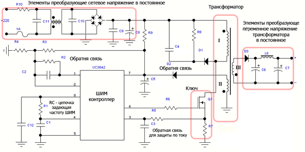
Что такое шим контроллер, как он устроен и работает, виды и схемы
Раньше для питания устройств использовали схему с понижающим (или повышающим, или многообмоточным) трансформатором, диодным мостом, фильтром для сглаживания пульсаций. Для стабилизации использовались линейные схемы на параметрических или интегральных стабилизаторах. Главным недостатком был низкий КПД и большой вес и габариты мощных блоков питания.
Во всех современных бытовых электроприборах используются импульсные блоки питания (ИБП, ИИП – одно и то же). В большинстве таких блоков питания в качестве основного управляющего элемента используют ШИМ-контроллер. В этой статье мы рассмотрим его устройство и назначение.
Содержание статьи
Определение и основные преимущества
ШИМ-контроллер – это устройство, которое содержит в себе ряд схемотехнических решений для управления силовыми ключами. При этом управление происходит на основании информации полученной по цепям обратной связи по току или напряжению – это нужно для стабилизации выходных параметров.
Иногда, ШИМ-контроллерами называются генераторы ШИМ-импульсов, но в них нет возможности подключить цепи обратной связи, и они подходят скорее для регуляторов напряжения, чем для обеспечения стабильного питания приборов. Однако в литературе и интернет-порталах часто можно встретить названия типа «ШИМ-контроллер, на NE555» или «… на ардуино» — это не совсем верно по вышеуказанным причинам, они могут использоваться только для регулирования выходных параметров, но не для их стабилизации.
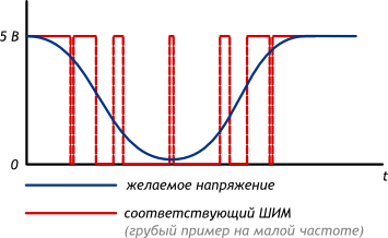
Аббревиатура «ШИМ» расшифровывается, как широтно-импульсная модуляция – это один из методов модуляции сигнала не за счёт величины выходного напряжения, а именно за счёт изменения ширины импульсов. В результате формируется моделируемый сигнал за счёт интегрирования импульсов с помощью C- или LC-цепей, другими словами – за счёт сглаживания.
Вывод: ШИМ-контроллер – устройство, которое управляет ШИМ-сигналом.
Научитесь разрабатывать устройства на базе микроконтроллеров и станьте инженером умных устройств с нуля: Инженер умных устройств
Основные характеристики
Для ШИМ-сигнала можно выделить две основных характеристики:
1. Частота импульсов – от этого зависит рабочая частота преобразователя. Типовыми являются частоты выше 20 кГц, фактически 40-100 кГц.
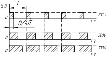
2. Коэффициент заполнения и скважность. Это две смежных величины характеризующие одно и то же. Коэффициент заполнения может обозначаться буквой S, а скважность D.
где T – это период сигнала,
Коэффициент заполнения – часть времени от периода, когда на выходе контроллера формируется управляющий сигнал, всегда меньше 1. Скважность всегда больше 1. При частоте 100 кГц период сигнала равен 10 мкс, а ключ открыт в течении 2.5 мкс, то коэффициент заполнения – 0.25, в процентах – 25%, а скважность равна 4.
Также важно учитывать внутреннюю конструкцию и предназначение по количеству управляемых ключей.
Отличия от линейных схем потери
Как уже было сказано, преимуществом перед линейными схемами у импульсных источников питания является высокий КПД (больше 80, а в настоящее время и 90%). Это обусловлено следующим:
Допустим сглаженное напряжение после диодного моста равно 15В, ток нагрузки 1А. Вам нужно получить стабилизированное питание напряжением 12В. Фактически линейный стабилизатор представляет собой сопротивление, которое изменяет свою величину в зависимости от величины входного напряжения для получения номинального выходного – с небольшими отклонениями (доли вольт) при изменениях входного (единицы и десятки вольт).
На резисторах, как известно, при протекании через них электрического тока выделяется тепловая энергия. На линейных стабилизаторах происходит такой же процесс. Выделенная мощность будет равна:
Так как в рассмотренном примере ток нагрузки 1А, входное напряжение 15В, а выходное – 12В, то рассчитаем потери и КПД линейного стабилизатора (КРЕНка или типа L7812):
Pпотерь=(15В-12В)*1А = 3В*1А = 3Вт
Тогда КПД равен:
Если же входное напряжение вырастит до 20В, например, то КПД снизится:
Основной особенностью ШИМ является то, что силовой элемент, пусть это будет MOSFET, либо открыт полностью, либо полностью закрыт и ток через него не протекает. Поэтому потери КПД обусловлены только потерями проводимости
И потерями переключения. Это тема для отдельной статьи, поэтому не будем останавливаться на этом вопросе. Также потери блока питания возникают в выпрямительных диодах (входных и выходных, если блок питания сетевой), а также на проводниках, пассивных элементах фильтра и прочем.
Общая структура
Рассмотрим общую структуру абстрактного ШИМ-контроллер. Я употребил слово «абстрактного» потому что, в общем, все они похожи, но их функционал все же может отличаться в определенных пределах, соответственно будет отличаться структура и выводы.
Внутри ШИМ-контроллера, как и в любой другой ИМС находится полупроводниковый кристалл, на котором расположена сложная схема. В состав контроллера входят следующие функциональные узлы:
1. Генератор импульсов.
2. Источник опорного напряжения. (ИОН)
3. Цепи для обработки сигнала обратной связи (ОС): усилитель ошибки, компаратор.
4. Генератор импульсов управляет встроенными транзисторами, которые предназначены для управления силовым ключом или ключами.
Количество силовых ключей, которыми может управлять ШИМ-контроллер, зависит от его предназначения. Простейшие обратноходовые преобразователи в своей схеме содержат 1 силовой ключ, полумостовые схемы (push-pull) — 2 ключа, мостовые — 4.
От типа ключа также зависит выбор ШИМ-контроллера. Для управления биполярным транзистором основным требованием является, чтобы выходной ток управления ШИМ-контроллера не был ниже, чем ток транзистора деленный на H21э, чтобы его включать и отключать достаточно просто подавать импульсы на базу. В этом случае подойдет большинство контроллеров.
В случае управления ключами с изолированным затвором (MOSFET, IGBT) есть определенные нюансы. Для быстрого отключения нужно разрядить емкость затвора. Для этого выходную цепь затвора выполняют из двух ключей — один из них соединен с источником питания с выводом ИМС и управляет затвором (включает транзистор), а второй установлен между выходом и землей, когда нужно отключить силовой транзистор — первый ключ закрывается, второй открывается, замыкая затвор на землю и разряжает его.
В некоторых ШИМ-контроллрах для маломощных блоков питания (до 50 Вт) силовые ключи встроенные и внешние не используются. Пример — 5l0830R
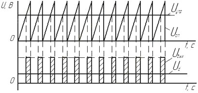
Если говорить обобщенно, то ШИМ-контроллер можно представить в виде компаратора, на один вход которого подан сигнал с цепи обратной связи (ОС), а на второй вход пилообразный изменяющийся сигнал. Когда пилообразный сигнал достигает и превышает по величине сигнал ОС, то на выходе компаратора возникает импульс.
При изменениях сигналов на входах ширина импульсов меняется. Допустим, что вы подключили мощный потребитель к блоку питания, и на его выходе напряжение просело, тогда напряжение ОС также упадет. Тогда в большей части периода будет наблюдаться превышение пилообразного сигнала над сигналом ОС, и ширина импульсов увеличится. Всё вышесказанное в определенной мере отражено на графиках.
Рабочая частота генератора устанавливается с помощью частотозадающей RC-цепи.
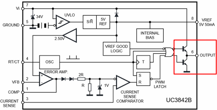
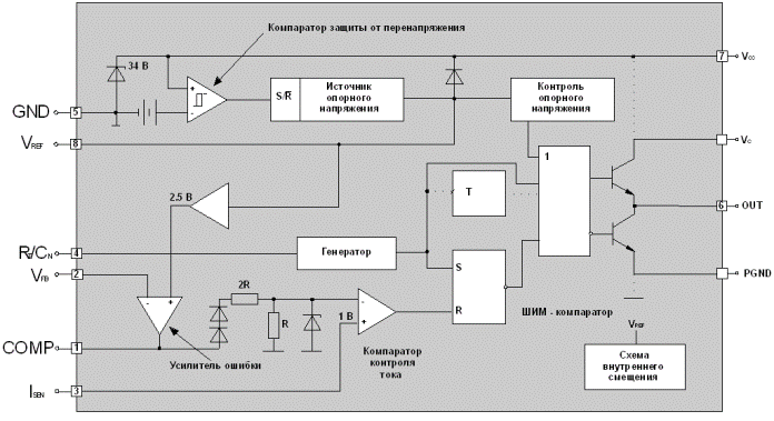
Функциональная схема ШИМ-контроллера на примере TL494, мы рассмотрим его позже подробнее. Назначение выводов и отдельных узлов описано в следующем подзаголовке.
Назначение выводов
ШИМ-контроллеры выпускаются в различных корпусах. Выводов у них может быть от трех до 16 и более. Соответственно от количества выводов, а вернее их назначения зависит гибкость использования контроллера. Например, в популярной микросхеме UC3843 — чаще всего 8 выводов, а в еще более культовой — TL494 — 16 или 24.
Поэтому рассмотрим типовые названия выводов и их назначение:
GND – общий вывод соединяется с минусом схемы или с землей.
Uc (Vc) – питание микросхемы.
Ucc (Vss, Vcc) – Вывод для контроля питания. Если питание проседает, то возникает вероятность того, что силовые ключи не будут полностью открываться, а из-за этого начнут греться и сгорят. Вывод нужен чтобы отключить контроллер в подобной ситуации.
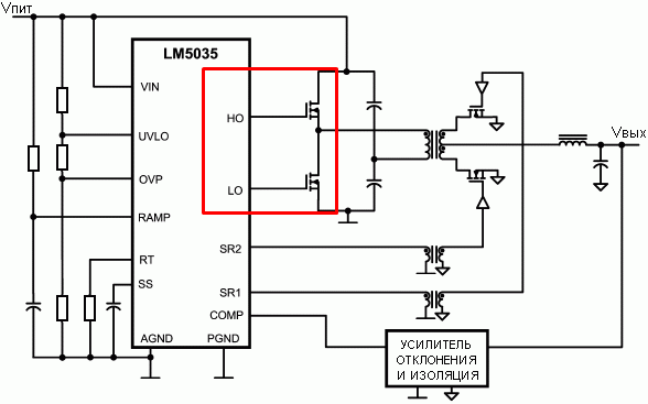
OUT – как видно из название — это выход контроллера. Здесь выводятся управляющий ШИМ-сигнал для силовых ключей. Выше мы упомянули, что в преобразователях разных топологий имеют разное количество ключей. Название вывода может отличаться в зависимости от этого. Например, в контроллерах для полумостовых схем он может называться HO и LO для верхнего и нижнего ключа соответственно. При этом и выход может быть однотактный и двухтактный (с одним ключем и двумя) — для управления полевыми транзисторами (пояснение см. выше). Но и сам контроллер может быть для однотактной и двухтактной схемы — с одним и двумя выходными выводами соответственно. Это важно.
Vref – опорное напряжения, обычно соединяется с землей через небольшой конденсатор (единицы микрофарад).
ILIM – сигнал с датчика тока. Нужен для ограничения выходного тока. Соединяется с цепями обратной связи.
ILIMREF – на ней устанавливается напряжение срабатывания ножки ILIM
SS – формируется сигнал для мягкого старта контроллера. Предназначен для плавного выхода на номинальный режим. Между ней и общим проводом для обеспечения плавного пуска устанавливают конденсатор.
RtCt – выводы для подключения времязадающей RC-цепи, которая определяет частоту ШИМ-сигнала.
CLOCK – тактовые импульсы для синхронизации нескольких ШИМ-контроллеров между собой тогда RC-цепь подключается только к ведущему контроллеру, а RT ведомых с Vref, CT ведомых соединяюся с общим.
RAMP – это ввод сравнения. На него подают пилообразное напряжение, например с вывода Ct, Когда оно превышает значение напряжение на выходе усиления ошибки, то на OUT появляется отключающий импульс — основа для ШИМ-регулирования.
INV и NONINV – это инвертирующий и неинвертирующий входы компаратора, на котором построен усилитель ошибки. Простыми словами: чем больше напряжении на INV — тем длинее выходные импульсы и наоборот. К нему подключается сигнал с делителя напряжения в цепи обратной связи с выхода. Тогда неинвертирующий вход NONINV подключают к общему проводу — GND.
EAOUT или Error Amplifier Output рус. Выход усилителя ошибки. Не смотря на то, что есть входы усилителя ошибки и с их помощью, в принципе можно регулировать выходные параметры, но контроллер довольно медленно на это реагирует. В результате медленной реакции может возникнуть возбуждение схемы, и она выйдет из строя. Поэтому с этого вывода через частотозависимые цепи подают сигналы на INV. Это еще называется частотной коррекцией усилителя ошибки.
Примеры реальных устройств
Для закрепления информации давайте рассмотрим несколько примеров типовых ШИМ-контроллеров и их схем включения. Мы будем делать это на примере двух микросхем:
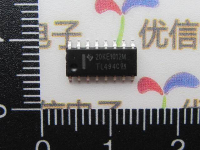
TL494 (её аналоги: KA7500B, КР1114ЕУ4, Sharp IR3M02, UA494, Fujitsu MB3759);
Они активно используются в блоках питания для компьютеров. Кстати, эти блоки питания обладают немалой мощностью (100 Вт и больше по 12В шине). Часто используются в качестве донора для переделки под лабораторный блок питания или универсальное мощное зарядное устройство, например для автомобильных аккумуляторов.
TL494 – обзор
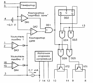
Начнем с 494-й микросхемы. Её технические характеристики:
В этом конкретном примере можно видеть большинство описанных выше выводов:
1. Неинвертирующий вход первого компаратора ошибки
2. Инвертирующий вход первого компаратора ошибки
3. Вход обратной связи
4. Вход регулировки мертвого времени
5. Вывод для подключения внешнего времязадающего конденсатора
6. Вывод для подключения времязадающего резистора
7. Общий вывод микросхемы, минус питания
8. Вывод коллектора первого выходного транзистора
9. Вывод эмиттера первого выходного транзистора
10. Вывод эмиттера второго выходного транзистора
11. Вывод коллектора второго выходного транзистора
12. Вход подачи питающего напряжения
13. Вход выбора однотактного или же двухтактного режима работы микросхемы
14. Вывод встроенного источника опорного напряжения 5 вольт
15. Инвертирующий вход второго компаратора ошибки
16. Неинвертирующий вход второго компаратора ошибки
На рисунке ниже изображен пример компьютерного блока питания на этой микросхеме.
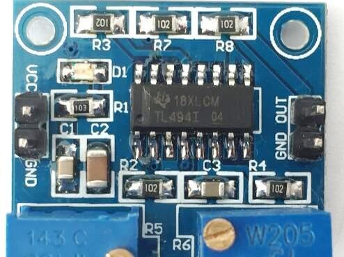
UC3843 — обзор
Другой популярной ШИМ является микросхема 3843 – на ней также строятся компьютерные и не только блоки питания. Её цоколевка расположена ниже, как вы можете наблюдать, у неё всего 8 выводов, но функции она выполняет те же, что и предыдущая ИМС.
Бывает UC3843 и в 14-ногом корпусе, но встречаются гораздо реже. Обратите внимание на маркировку – дополнительные выводы либо дублируются, либо незадействованы (NC).
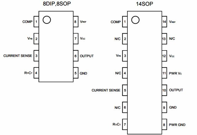
Расшифруем назначением выводов:
1. Вход компаратора (усилителя ошибки).
2. Вход напряжения обратной связи. Это напряжение сравнивается с опорным внутри ИМС.
3. Датчик тока. Подключается к резистору стоящему в между силовым транзистором и общим проводом. Нужен для защиты от перегрузок.
4. Времязадающая RC-цепь. С её помощью задаётся рабочая частота ИМС.
6. Выход. Управляющее напряжение. Подключается к затвору транзистора, здесь двухтактный выходной каскад для управления однотактным преобразователем (одним транзистором), что можно наблюдать на рисунке ниже.
7. Напряжение питания микросхемы.
8. Выход источника опорного напряжения (5В, 50 мА).
Её внутренняя структура.
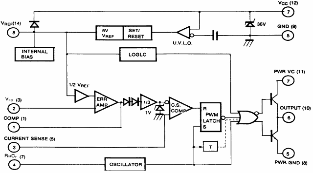
Можно убедится, что во многом похожа и на другие ШИМ-контроллеры.
Простая схема сетевого источника питания на UC3842
Явно полезное:
ШИМ со встроенным силовым ключем
ШИМ-контроллеры со встроенным силовым ключем используются как в трансформаторных импульсных блоках питания, так и в бестрансформаторных DC-DC преобразователях понижающего (Buck), повышающего (Boost) и понижающее-повышающего (Buck-Boost) типов.
Пожалуй, одним из наиболее удачных примеров будет распространенная микросхема LM2596, на базе которого на рынке можно найти массу таких преобразователей, как изображен ниже.
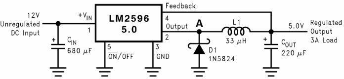
Такая микросхема содержит в себе все вышеописанные технические решения, а также вместо выходного каскада на маломощных ключах в ней встроен силовой ключ, способный выдержать ток до 3А. Ниже изображена внутренняя структура такого преобразователя.
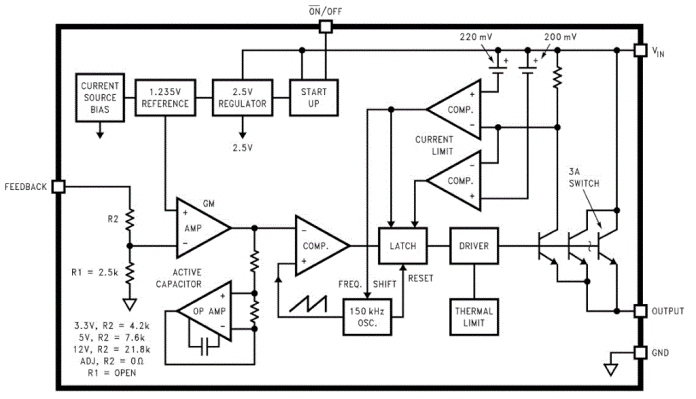
Можно убедиться, что в сущности особых отличий от рассмотренных в ней нет.
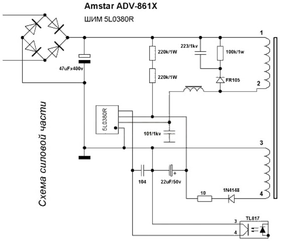
А вот пример трансформаторного блока питания для светодиодной ленты на подобном контроллере, как видите силового ключа нет, а только микросхема 5L0380R с четырьмя выводами. Отсюда следует, что в определенных задачах сложная схемотехника и гибкость TL494 просто не нужна. Это справедливо для маломощных блоков питания, где нет особых требований к шумам и помехам, а выходные пульсации можно погасить LC-фильтром. Это блок питания для светодиодных лент, ноутбуков, DVD-плееров и прочее.
Заключение
В начале статьи было сказано о том, что ШИМ-контроллер это устройство которое моделирует среднее значение напряжения за счет изменения ширина импульсов на основании сигнала с цепи обратной связи. Отмечу, что названия и классификация у каждого автора часто отличается, иногда ШИМ-контроллером называют простой ШИМ-регулятор напряжения, а описанное в этой статьей семейство электронных микросхем называют «Интегральная подсистема для импульсных стабилизированных преобразователей». От названия суть не меняется, но возникают споры и недопонимания.
Надеюсь, что эта статья была для вас полезной. Смотрите также другие статьи в категории Электрическая энергия в быту и на производстве » Практическая электроника
Источник


Усилитель ошибки наиболее часто встречающийся в схемах управления с обратной связью однонаправленного напряжения, когда выходное напряжение пробы цепи под контролем, подаются обратно и сравнивается с опорным напряжением стабильной. Любая разница между ними создает компенсирующее напряжение ошибки, которое стремится сдвинуть выходное напряжение в соответствии с проектной спецификацией.
Усилитель ошибки — это, по сути, то, о чем говорится в его названии, то есть он усиливает сигнал ошибки. Эта ошибка основана на разнице между опорным сигналом и входным сигналом. Его также можно рассматривать как разницу между двумя входами. Они обычно используются вместе с петлями обратной связи из-за их механизма самокоррекции. У них есть инвертирующий и неинвертирующий набор входных контактов, который отвечает за то, чтобы выходной сигнал был разностью входов.
Устройства
- Дискретные транзисторы
- Операционные усилители
Приложения
- Регулируемый блок питания .
- Усилители мощности постоянного тока
- Измерительное оборудование
- Сервомеханизмы
Смотрите также
- Дифференциальный усилитель
внешние ссылки
- Разработка и применение усилителя ошибок, alphascientific.com . Первоначально просмотрено 27 апреля 2009 г., сейчас 404. Попробуйте https://web.archive.org/web/20081006222215/http://www.alphascientific.com/technotes/technote3.pdf
- Усилитель ошибки как элемент регулятора напряжения : анализ устойчивости линейных регуляторов с малым падением напряжения
с проходным элементом PMOS
|
|
This article includes a list of references, related reading or external links, but its sources remain unclear because it lacks inline citations. Please help to improve this article by introducing more precise citations. (October 2021) (Learn how and when to remove this template message) |
Internal structure
Application
An error amplifier is most commonly encountered in feedback unidirectional voltage control circuits, where the sampled output voltage of the circuit under control, is fed back and compared to a stable reference voltage. Any difference between the two generates a compensating error voltage which tends to move the output voltage towards the design specification.
An error amplifier is essentially what its name says, that is, it amplifies an error signal. This error is based on the difference between a reference signal and the input signal. It can also be treated as the difference between the two inputs. These are usually used in unison with feedback loops, owing to their self-correcting mechanism. They have an inverting and a non-inverting input pin set, which is what is responsible for the output to be the difference of the inputs.
Devices[edit]
- Discrete Transistors
- Operational amplifiers
Applications[edit]
- Regulated power supply.
- D.C Power Amplifiers
- Measurement Equipment
- Servomechanisms
See also[edit]
- Differential amplifier
External links[edit]
- Error Amplifier Design and Application Archived 28 March 2018 at the Wayback Machine, alphascientific.com. Originally accessed 27 April 2009, now 404. Try https://web.archive.org/web/20081006222215/http://www.alphascientific.com/technotes/technote3.pdf
- Error amplifier as an element in a voltage regulator:
Stability analysis of low-dropout linear regulators with a PMOS pass element Archived 7 July 2011 at the Wayback Machine
|
This electronics-related article is a stub. You can help Wikipedia by expanding it. |
- v
- t
- e
- error amplifier
-
усилитель сигнала ошибки
Англо русский политехнический словарь.
.
2011.
Смотреть что такое «error amplifier» в других словарях:
-
Error amplifier (electronics) — An error amplifier is most commonly encountered in feedback unidirectional voltage control circuits where the sampled output voltage of the circuit under control is fed back and compared to a stable reference voltage. Any difference between the… … Wikipedia
-
Current-feedback operational amplifier — Representative schematic of a current feedback op amp or amplifier. The current feedback operational amplifier otherwise known as CfoA or CfA is a type of electronic amplifier whose inverting input is sensitive to current, rather than to voltage… … Wikipedia
-
Operational amplifier applications — This article illustrates some typical applications of operational amplifiers. A simplified schematic notation is used, and the reader is reminded that many details such as device selection and power supply connections are not shown. Contents 1… … Wikipedia
-
Logarithmic video amplifier — A logarithmic video amplifier or LVA is typically part of radar and electronic countermeasures microwave systems and sonar navigation systems, used to convert a very large dynamic range input power to an output voltage that increases… … Wikipedia
-
Class-D amplifier — Block diagram of a basic switching or PWM (class D) amplifier A class D amplifier or switching amplifier is an electronic amplifier where all power devices (usually MOSFETs) are operated as binary switches. They are either fully on or fully… … Wikipedia
-
Electronic amplifier — A practical amplifier circuit An electronic amplifier is a device for increasing the power of a signal. It does this by taking energy from a power supply and controlling the output to match the input signal shape but with a larger amplitude. In… … Wikipedia
-
Operational amplifier — A Signetics μa741 operational amplifier, one of the most successful op amps. An operational amplifier ( op amp ) is a DC coupled high gain electronic voltage amplifier with a differential input and, usually, a single ended output.[1] An op amp… … Wikipedia
-
Valve audio amplifier — A valve (UK) audio amplifier or vacuum tube (US) audio amplifier is a valve amplifier used for sound recording, reinforcement, or reproduction. Until the invention of solid state devices such as the transistor, all electronic amplification was… … Wikipedia
-
AN/FPS-16 — manned space program and the U.S. Air Force. The accuracy of Radar Set AN/FPS 16 is such that the position data obtained from point source targets has azimuth and elevation angular errors of less than 0.1 milliradian (approximately 0.006 degree)… … Wikipedia
-
YEA — YES vote (Governmental » Military) YES vote (Governmental » US Government) YES vote (Governmental » United Nations) * Young Entrepreneurs Asia (Business » Firms) * Youth Educational Adventures (Community » Educational) * Yaw Error Amplifier… … Abbreviations dictionary
-
Low dropout regulator — A low dropout or LDO regulator is a DC linear voltage regulator which can operate with a very small input output differential voltage. The main components are a power FET and a differential amplifier (error amplifier). One input of the… … Wikipedia
Theoritical considerations for buck mode switching regulators
Carl Nelson, in Analog Circuit Design, 2013
Error Amplifier
The error amplifier in Figure 11 is a single stage design with added inverters to allow the output to swing above and below the common mode input voltage. One side of the amplifier is tied to a trimmed internal reference voltage of 2.21V. The other input is brought out as the FB (feedback) pin. This amplifier has a GM (voltage in to current out) transfer function of ∼5000μmho. Voltage gain is determined by multiplying GM times the total equivalent output loading, consisting of the output resistance of Q4 and Q6 in parallel with the series RC external frequency compensation network. At DC, the external RC is ignored, and with a parallel output impedance for Q4 and Q6 of 400kΩ, voltage gain is ≈2000. At frequencies above a few hertz, voltage gain is determined by the external compensation, RC and CC.

Figure 11. Error Amplifier
AV=Gm2π•f•CCat mid-frequenciesAV=Gm•RCat high frequencies
Phase shift from the FB pin to the VC pin is 90° at mid-frequencies where the external CC is controlling gain, then drops back to 0° (actually 180° since FB is an inverting input) when the reactance of CC is small compared to RC. The low frequency “pole” where the reactance of CC is equal to the output impedance of Q4 and Q6 (r0), is:
FPOLE=12π•r0•Cr0≈400kΩ
Although fPOLE varies as much as 3:1 due to r0 variations, mid-frequency gain is dependent only on GM, which is specified much tighter on the data sheet. The higher frequency “zero” is determined solely by RC and CC:
fZERO=12π•RC•CC
The error amplifier has asymmetrical peak output current. Q3 and Q4 current mirrors are unity gain, but the Q6 mirror has a gain of 1.8 at output null and a gain of 8 when the FB pin is high (Q1 current = 0). This results in a maximum positive output current of 140μA and a maximum negative (sink) output current of =1.1mA. The asymmetry is deliberate—it results in much less regulator output overshoot during rapid start-up or following the release of an output overload. Amplifier offset is kept low by area scaling Q1 and Q2 at 1.8:1.
Amplifier swing is limited by the internal 5.8V supply for positive outputs and by D1 and D2 when the output goes low. Low clamp voltage is approximately one diode drop (−0.7V – 2mV/°C).
Note that both the FB pin and the VC pin have other internal connections. Refer to the frequency shifting and synchronizing discussions.
Read full chapter
URL:
https://www.sciencedirect.com/science/article/pii/B9780123978882000055
Linear regulator
Keng C. Wu, in Power Electronic System Design, 2021
8.1.1.1 Open loop
Surrounding the error amplifier and the output feedback divider, R1 and R2, the inverting input node, Vn, and the noninverting node, Vp, voltages are
(8.1)Vn=R2R1+R2Vo+Vos+R1R2R1+R2Ib,Vp=Vref
The error amplifier output therefore gives
(8.2)V2=A(Vp−Vn)=A(Vref−R2R1+R2Vo−Vos−R1R2R1+R2Ib)
The base-emitter loop of transistor Q1 gives
(8.3)R3IB1+Vbe1+R4(1+hFE1)IB1=V2,approximationIB1=ISeV2−[R3+(1+hFE1)R4]IB1VT,exact
The exact expression invokes transistor p-n junction saturation current, Is, and thermal voltage, VT.
In other words, the Q1 base current (approximation) is
(8.4)IB1=V2−Vbe1R3+R4(1+hFE1)=A(Vref−R2R1+R2Vo−Vos−R1R2R1+R2Ib)−Vbe1R3+R4(1+hFE1)
And the Q2 base current (approximation) is
(8.5)IB2=hFE1IB1−Vbe2R5=hFE1A(Vref−R2R1+R2Vo−Vos−R1R2R1+R2Ib)−Vbe1R3+R4(1+hFE1)−Vbe2R5
Clearly, the output voltage is translated to a control current that is responsible for regulating the output given a known reference, Vref. This concludes the first part.
The other part, power train, yields
(8.6)Vo=(R1+R2)RLR1+R2+RLIC2=(R1+R2)RLR1+R2+RLhFE2·IB2Vi=Vce+Vo
where Vce is the collector-to-emitter drop.
Read full chapter
URL:
https://www.sciencedirect.com/science/article/pii/B9780323885423000017
Current-Fed Converter
Keng Wu, in Power Converters with Digital Filter Feedback Control, 2016
10.5 I-fed converter with digital control
The analog error amplifier identified in Section 10.3, following the modulator gain evaluation, is transformed to the z-domain with a bilinear transformation constant C = 2 MHz (converter switching frequency 100 kHz, sampling frequency 1 MHz, transform constant = twice of sampling). The resulting z-domain digital filter function is in the form of (1.23) with these coefficients,
a0=7.451×10⁻⁴a1=−7.337×10⁻⁴a2=−7.451×10⁻⁴a3=7.338×10⁻⁴ b1=−2.959b2=2.919b3=−0.96
Figure 10.7a–d shows the SIMULINK schematic with digital filter and performance in time domain.


Figure 10.7. SIMULINK Schematic with Digital Filter.
(a) Inductor current, (b) secondary current, (c) output voltage, and (d) input current.
Read full chapter
URL:
https://www.sciencedirect.com/science/article/pii/B9780128042984000101
Feedback Loop Analysis and Stability
Sanjaya Maniktala, in Switching Power Supplies A — Z (Second Edition), 2012
Pulse-Width Modulator Transfer Function
The output of the error amplifier (sometimes called “COMP,” sometimes “EA-out,” sometimes “control voltage”) is applied to one of the inputs of the PWM comparator. This is the terminal marked “Control” in Figures 12.9 and 12.10. On the other input of this PWM comparator, we apply a sawtooth voltage ramp — either internally generated from the clock when using “voltage-mode control,” or derived from the current ramp when using “current-mode control” (explained later). Thereafter, by standard comparator action, we get pulses of desired width with which to drive the switch.
Since the feedback signal coming from the output rail of the power supply goes to the inverting input of the error amplifier, if the output is below the set regulation level, the output of the error amplifier goes high. This causes the PWM to increase the pulse width (duty cycle) and thus try to make the output voltage rise. Similarly, if the output of the power supply goes above its set value, the error amplifier output goes low, causing the duty cycle to decrease (see upper third of Figure 12.11).
As mentioned previously, the output of the PWM stage is duty cycle, and its input is the “control voltage” or the “EA-out.” So, as we said, the gain of this stage is not a dimensionless quantity, but has units of 1/V. From the middle of Figure 12.11, we can see that this gain is equal to 1/VRAMP, where VRAMP is the peak-to-peak amplitude of the ramp sawtooth.
Read full chapter
URL:
https://www.sciencedirect.com/science/article/pii/B9780123865335000127
DCM Boost Converter with Voltage-Mode Control
Keng Wu, in Power Converters with Digital Filter Feedback Control, 2016
7.6 Conversion to digital control
We now want to convert the analog error amplifier, EA(s), identified in Section 7.4, to its digital equivalent H(z). It turns out that some property not well understood, at least to this author, exists. From the EA(ω) plot in frequency domain, 100 kHz sampling was thought to be a good choice, but it ends up having a frequency response, H(ω), that is utterly incompatible as shown in Figure 7.8, with the analog version.

Figure 7.8. Incompatible Digital Filter Sampled at 100 kHz.
Increasing the sampling frequency to 300 kHz improves matching, Figure 7.9, with losses in high frequency.

Figure 7.9. Improved Matching at 300 kHz Sampling.
Increasing the sampling frequency further to 800 kHz improves more, Figure 7.10, but further increase to 900 kHz makes it worse. We therefore settle for sampling at 800 kHz.

Figure 7.10. Better Matching at High Frequency with 800 kHz Sampling.
At 800 kHz sampling, the polynomial coefficients for the corresponding HII(z), (1.19), is given as,
a0=5.392×10⁻³a1=38.663×10⁻⁶a2=−5.353×10⁻³ b1=−1.991×10−0b2=991.465×10⁻³
With the digital filter identified, Figure 7.1 is transformed to its digital control version, Figure 7.11. The digital filter is also proved to be stable, Figure 7.12, with poles within the unit circle of z-plane.

Figure 7.11. Boost Converter with Digital Filter in Feedback Loop.

Figure 7.12. Digital Filter is Stable.
Read full chapter
URL:
https://www.sciencedirect.com/science/article/pii/B9780128042984000071
Forward Converter with Voltage-Mode Control
Keng Wu, in Power Converters with Digital Filter Feedback Control, 2016
1.7 Other approaches and considerations
In the process of converting an analog error amplifier to digital in Section 1.4, the bilinear transform was invoked. The transform is considered valid, based on the fact of acceptable mathematical approximation alone. It does not take into consideration its physical significance. Briefly, in particular the choice of constant C, there were many choices, none perfect. One approach attempts to match both at a single, chosen frequency. In another, the responses of both versions across a low frequency band are made almost equal. Both efforts set an eye on the performance in the frequency domain. There are alternatives, of course, and that is changing the focus to the time domain. One is called impulse invariance method. It implies that the impulse response of a digital filter is forced to be identical to the impulse of its analog counterpart. It is basically a procedural matter that does not require cumbersome theoretical support. We outline only the process here and will give a demonstration later in an example.
Three steps are called for in the impulse invariance method. Step one takes the inverse Laplace transform of the analog compensator function (inverting sign excluded), identified by way of Section 1.3. This yields the time-domain impulse response of the corresponding analog amplifier. Step two takes z-transform of the impulse response function in the time domain. Then the last step follows by arranging the z-domain function in the form of (1.24).
In the analog world, circuit operations and performances are sensitive to the value of components. Digital filters obtained through the above fare even worse by the fact of (1.17), (1.19), (1.20), and (1.23). The performance of a digital filter is extremely sensitive to the coefficients of its numerator and denominator polynomial. Readers are strongly advised to retain coefficients’ numerical precision to at the least 10 decimal places.
The last, but not the least, concern is the local stability of the compensator. Poles of HII(z) in (1.19), HIII(z) in (1.23), or in general, H(z) of (1.24), must lie within the unit circle in the z-plane. We will see to it in the example to follow.
Read full chapter
URL:
https://www.sciencedirect.com/science/article/pii/B9780128042984000010
Forward Converter with Current-Mode Control
Keng Wu, in Power Converters with Digital Filter Feedback Control, 2016
2.5 Matlab SIMULINK simulation
In both Figures 2.1 and 2.2, a type-III error amplifier was employed for demonstration purpose as well as for a 60°-phase margin. It turns out that if the desired phase margin is reduced to 45° at the same crossover frequency of 10 kHz, a type-II error amplifier with two less components can perform just as well for current-mode control. The reader is invited to confirm, with R1a = 2K preselected, C1a = 0.0029 μF, C2a = 0.009 μF, and R2a = 3.6K. In the depictedSIMULINK models, type-II error amplifiers are shown. Figure 2.12 gives a physical device model and Figure 2.12a–h present simulation plots. Figure 2.13 replaces the physical model with continuous transfer function H(s), while Figure 2.14 plugs in the corresponding digital filter.


Figure 2.12. SIMULINK Model with Error Amp Represented by Physical Device.
(a) Output voltage, (b) error voltage, (c) D1 and D2 cathode, (d) input current, (e) switch current, (f) inductor current, (g) D1 current, (h) D2 current.


Figure 2.13. SIMULINK Model with Error Amp in H(s) Form.
(a) Output voltage. (b) error voltage. (c) D1 and D2 cathode. (d) input current. (e) switch current. (f) inductor current. (g) D1 current. (h) D2 current.


Figure 2.14. SIMULINK Model with Error Amp in Hz Form.
(a) Output voltage, (b) error voltage, (c) D1 and D2 cathode, (d) input current. (e) switch current, (f) inductor current, (g) D1 current, (h) D2 current.
Read full chapter
URL:
https://www.sciencedirect.com/science/article/pii/B9780128042984000022
Switch-mode DC/DC converters
Keng C. Wu, in Power Electronic System Design, 2021
9.14 Close loop—digital
So far, the key controller; which is the error amplifier identified as, for instance, EA(s) in Fig. 9.66; remains entirely in analog forms using analog integrated circuits and passive RC components. This fact had also held true for decades covering the invention of black/white TV, color TV, audio cassette tape, VCR, etc. and later improvements of those products. Then, perhaps in early 1980s, devices with discrete recording and readout, not digital yet, began to show up. Discrete signal is basically just a sampled, discontinuous staircase approximation of its analog counterpart. While a true digital signal further represents each and every discrete sample in stream of binary 0/1 format including synchronization, identification, data, encryption, action, error correction, etc. With the advance of understanding in digital signal processing starting in early 1970s and mostly limited to post processing, instead of real time, early 1980s also saw some bright minds beginning to probe the possibility of digital filter and control for power converters. However, after almost 40 years, the progress is far from satisfactory. As late as 2017, published material discussing power processing with digital feedback still carried significant misconceptions, or errors.
On Oct. 26, 2017, at the invitation of Electronic Design, Penton Publication (On-Line version), this author published “A Step-by-Step Primer on Digital Power-Supply Design”; [http://www.electronicdesign.com/power/step-step-primer-digital-power-supply-design].
Considering the article length and the standing alone nature, it is included as an appendix; Appendix I.
Read full chapter
URL:
https://www.sciencedirect.com/science/article/pii/B9780323885423000030
LT1070 design manual
Carl Nelson, in Analog Circuit Design, 2011
Feedback pin
The feedback pin is the inverting input to a single stage error amplifier. The noninverting input to this amplifier is internally tied to a 1.244V reference as shown in Figure 5.4.

Figure 5.4.
Input bias current of the amplifier is typically 350nA with the output of the amplifier in its linear region. The amplifier is a gm type, meaning that it has high output impedance with controlled voltage-to-current gain (gm ≈ 4400μmhos). DC voltage gain with no load is ≈ 800.
The feedback pin has a second function; it is used to program the LT1070 for normal or flyback-regulated operation (see description of block diagram). In Figure 5.4, Q53 is biased with a base voltage approximately 1V. This clamps the feedback pin to about 0.4V when current is drawn out of the pin. A current of ≈10μA or higher through Q53 forces the regulator to switch from normal operation to flyback mode, but this threshold current can vary from 3μA to 30μA. The LT1070 is in flyback mode during normal start-up until the feedback pin rises above 0.45V. The resistor divider used to set output voltage will draw current out of the feedback pin until the output voltage is up to about 33% of its regulated value.
If it is desired to run the LT1070 in the fully isolated flyback mode, a single resistor is tied from the feedback pin to ground. The feedback pin then sits at a voltage of ≈ 0.4V for R = 8.2k. The actual voltage depends on resistor value since the feedback pin has about 200Ω output impedance in this mode. 500μA in the resistor will drop the feedback pin voltage from 0.4V to 0.3V. Minimum current through the resistor to guarantee flyback operation is 50μA. Actual resistor value is chosen to fine-trim flyback regulated voltage. (See discussion of isolated flyback mode operation and graphs of feedback pin characteristics.)
An internal 30Ω resistor and 5.6V Zener protect the feedback pin from overvoltage stress. Maximum transient voltage is ±15V. This high transient condition most commonly occurs during fast fall time output shorts if a feedforward capacitor is used around the feedback divider. If a feedforward capacitor is used for DC output voltages greater than 15V, a resistor equal to VOUT/20mA should be used between the divider node and the feedback pin as shown in Figure 5.5.

Figure 5.5.
Keep in mind when using the LT1070 that the feedback pin reference voltage is referred to the ground pin of the regulator, and the ground pin can have switch currents exceeding 5A. Any resistance in the ground pin connection will degrade load regulation. Best regulation is obtained by tying the grounded end of the feedback divider directly to the ground pin of the LT1070, as a separate connection from the power ground. This limits output voltage errors to just the drop across the ground pin resistance instead of multiplying it by the feedback divider ratio. See discussion of ground pin.
Read full chapter
URL:
https://www.sciencedirect.com/science/article/pii/B9780123851857000056
Space Interference
Reinaldo Perez, in Wireless Communications Design Handbook, 1998
4.6.7.2 Transient Effects in SMPSs
In the simplified circuit of a switching-mode power supply, an error amplifier compares output voltage Vout with a reference Vref and controls the duty cycle, D, via a pulse width modulator as shown in Figure 4.32. The output capacitor Cout is represented by its equivalent circuit that includes the equivalent series resistance (ESR) and the equivalent series inductance (ESL). When we have a load step δI, current through the choke inductance L cannot be instantly changed. There will always be a finite time t needed for L to accommodate δI, given by the expression

Figure 4.32. Simplified diagram of an SMPS with output capacitor model (ESR & ESL).
(4.10)t>LδIVinDmax−Vout−Vdiode,
where Dmax is the maximum duty cycle and Vdiode is the diode’s voltage drop. The choke current Ichoke slews to the new load current, but before it does that Iload flows through Cout. This results in an output voltage deviation δVout that may be as much as
(4.11)δVout≤ESLdIloaddt+ESRδI,
where dIload/dt is the load’s current slew rate (A/sec).The SMPS’s Cout acts as a reservoir for these current transients. The delay that is observed is compounded by the wiring and possible long traces in the PCB. As can be observed in Figure 4.32, traces have self-inductances and resistances, and when Iload changes from Faraday’s law, Lwire/trace will cause an initial voltage deviation δV given by
(4.12)δV=−Lwire/tracesdIloaddt.
Furthermore, Rwire/trace will cause an input voltage drop as Iload slews. The time that is needed to change a current through load wires/traces in a PCB is given by
(4.13)t=tdelay+trise,
where tdelay is the SMPS delay time and trise is the time needed for Iwire/traces to catch up to the load current, given by
(4.14)trise=tdelaydIload/dtVmax−VloadLwire/trace−dIloaddt
where Vmax is the maximum output voltage during the transient recovery of the supply. The output load will experience a dip of as much as
(4.15)δVout=ESRtdIloaddt+t2dIload/dtCload.
A computer simulation of a circuit of the type shown in Figure 4.32 using SPICE can show the effects of load wire/traces, inductances, and external capacitance, as shown in Figure 4.33.

Figure 4.33. Load transients resulting from modeling output loads of an SMPS.
Read full chapter
URL:
https://www.sciencedirect.com/science/article/pii/S1874610199800179
Theoritical considerations for buck mode switching regulators
Carl Nelson, in Analog Circuit Design, 2013
Error Amplifier
The error amplifier in Figure 11 is a single stage design with added inverters to allow the output to swing above and below the common mode input voltage. One side of the amplifier is tied to a trimmed internal reference voltage of 2.21V. The other input is brought out as the FB (feedback) pin. This amplifier has a GM (voltage in to current out) transfer function of ∼5000μmho. Voltage gain is determined by multiplying GM times the total equivalent output loading, consisting of the output resistance of Q4 and Q6 in parallel with the series RC external frequency compensation network. At DC, the external RC is ignored, and with a parallel output impedance for Q4 and Q6 of 400kΩ, voltage gain is ≈2000. At frequencies above a few hertz, voltage gain is determined by the external compensation, RC and CC.
Figure 11. Error Amplifier
AV=Gm2π•f•CCat mid-frequenciesAV=Gm•RCat high frequencies
Phase shift from the FB pin to the VC pin is 90° at mid-frequencies where the external CC is controlling gain, then drops back to 0° (actually 180° since FB is an inverting input) when the reactance of CC is small compared to RC. The low frequency “pole” where the reactance of CC is equal to the output impedance of Q4 and Q6 (r0), is:
FPOLE=12π•r0•Cr0≈400kΩ
Although fPOLE varies as much as 3:1 due to r0 variations, mid-frequency gain is dependent only on GM, which is specified much tighter on the data sheet. The higher frequency “zero” is determined solely by RC and CC:
fZERO=12π•RC•CC
The error amplifier has asymmetrical peak output current. Q3 and Q4 current mirrors are unity gain, but the Q6 mirror has a gain of 1.8 at output null and a gain of 8 when the FB pin is high (Q1 current = 0). This results in a maximum positive output current of 140μA and a maximum negative (sink) output current of =1.1mA. The asymmetry is deliberate—it results in much less regulator output overshoot during rapid start-up or following the release of an output overload. Amplifier offset is kept low by area scaling Q1 and Q2 at 1.8:1.
Amplifier swing is limited by the internal 5.8V supply for positive outputs and by D1 and D2 when the output goes low. Low clamp voltage is approximately one diode drop (−0.7V – 2mV/°C).
Note that both the FB pin and the VC pin have other internal connections. Refer to the frequency shifting and synchronizing discussions.
Read full chapter
URL:
https://www.sciencedirect.com/science/article/pii/B9780123978882000055
Linear regulator
Keng C. Wu, in Power Electronic System Design, 2021
8.1.1.1 Open loop
Surrounding the error amplifier and the output feedback divider, R1 and R2, the inverting input node, Vn, and the noninverting node, Vp, voltages are
(8.1)Vn=R2R1+R2Vo+Vos+R1R2R1+R2Ib,Vp=Vref
The error amplifier output therefore gives
(8.2)V2=A(Vp−Vn)=A(Vref−R2R1+R2Vo−Vos−R1R2R1+R2Ib)
The base-emitter loop of transistor Q1 gives
(8.3)R3IB1+Vbe1+R4(1+hFE1)IB1=V2,approximationIB1=ISeV2−[R3+(1+hFE1)R4]IB1VT,exact
The exact expression invokes transistor p-n junction saturation current, Is, and thermal voltage, VT.
In other words, the Q1 base current (approximation) is
(8.4)IB1=V2−Vbe1R3+R4(1+hFE1)=A(Vref−R2R1+R2Vo−Vos−R1R2R1+R2Ib)−Vbe1R3+R4(1+hFE1)
And the Q2 base current (approximation) is
(8.5)IB2=hFE1IB1−Vbe2R5=hFE1A(Vref−R2R1+R2Vo−Vos−R1R2R1+R2Ib)−Vbe1R3+R4(1+hFE1)−Vbe2R5
Clearly, the output voltage is translated to a control current that is responsible for regulating the output given a known reference, Vref. This concludes the first part.
The other part, power train, yields
(8.6)Vo=(R1+R2)RLR1+R2+RLIC2=(R1+R2)RLR1+R2+RLhFE2·IB2Vi=Vce+Vo
where Vce is the collector-to-emitter drop.
Read full chapter
URL:
https://www.sciencedirect.com/science/article/pii/B9780323885423000017
Current-Fed Converter
Keng Wu, in Power Converters with Digital Filter Feedback Control, 2016
10.5 I-fed converter with digital control
The analog error amplifier identified in Section 10.3, following the modulator gain evaluation, is transformed to the z-domain with a bilinear transformation constant C = 2 MHz (converter switching frequency 100 kHz, sampling frequency 1 MHz, transform constant = twice of sampling). The resulting z-domain digital filter function is in the form of (1.23) with these coefficients,
a0=7.451×10⁻⁴a1=−7.337×10⁻⁴a2=−7.451×10⁻⁴a3=7.338×10⁻⁴ b1=−2.959b2=2.919b3=−0.96
Figure 10.7a–d shows the SIMULINK schematic with digital filter and performance in time domain.
Figure 10.7. SIMULINK Schematic with Digital Filter.
(a) Inductor current, (b) secondary current, (c) output voltage, and (d) input current.
Read full chapter
URL:
https://www.sciencedirect.com/science/article/pii/B9780128042984000101
Feedback Loop Analysis and Stability
Sanjaya Maniktala, in Switching Power Supplies A — Z (Second Edition), 2012
Pulse-Width Modulator Transfer Function
The output of the error amplifier (sometimes called “COMP,” sometimes “EA-out,” sometimes “control voltage”) is applied to one of the inputs of the PWM comparator. This is the terminal marked “Control” in Figures 12.9 and 12.10. On the other input of this PWM comparator, we apply a sawtooth voltage ramp — either internally generated from the clock when using “voltage-mode control,” or derived from the current ramp when using “current-mode control” (explained later). Thereafter, by standard comparator action, we get pulses of desired width with which to drive the switch.
Since the feedback signal coming from the output rail of the power supply goes to the inverting input of the error amplifier, if the output is below the set regulation level, the output of the error amplifier goes high. This causes the PWM to increase the pulse width (duty cycle) and thus try to make the output voltage rise. Similarly, if the output of the power supply goes above its set value, the error amplifier output goes low, causing the duty cycle to decrease (see upper third of Figure 12.11).
As mentioned previously, the output of the PWM stage is duty cycle, and its input is the “control voltage” or the “EA-out.” So, as we said, the gain of this stage is not a dimensionless quantity, but has units of 1/V. From the middle of Figure 12.11, we can see that this gain is equal to 1/VRAMP, where VRAMP is the peak-to-peak amplitude of the ramp sawtooth.
Read full chapter
URL:
https://www.sciencedirect.com/science/article/pii/B9780123865335000127
DCM Boost Converter with Voltage-Mode Control
Keng Wu, in Power Converters with Digital Filter Feedback Control, 2016
7.6 Conversion to digital control
We now want to convert the analog error amplifier, EA(s), identified in Section 7.4, to its digital equivalent H(z). It turns out that some property not well understood, at least to this author, exists. From the EA(ω) plot in frequency domain, 100 kHz sampling was thought to be a good choice, but it ends up having a frequency response, H(ω), that is utterly incompatible as shown in Figure 7.8, with the analog version.
Figure 7.8. Incompatible Digital Filter Sampled at 100 kHz.
Increasing the sampling frequency to 300 kHz improves matching, Figure 7.9, with losses in high frequency.
Figure 7.9. Improved Matching at 300 kHz Sampling.
Increasing the sampling frequency further to 800 kHz improves more, Figure 7.10, but further increase to 900 kHz makes it worse. We therefore settle for sampling at 800 kHz.
Figure 7.10. Better Matching at High Frequency with 800 kHz Sampling.
At 800 kHz sampling, the polynomial coefficients for the corresponding HII(z), (1.19), is given as,
a0=5.392×10⁻³a1=38.663×10⁻⁶a2=−5.353×10⁻³ b1=−1.991×10−0b2=991.465×10⁻³
With the digital filter identified, Figure 7.1 is transformed to its digital control version, Figure 7.11. The digital filter is also proved to be stable, Figure 7.12, with poles within the unit circle of z-plane.
Figure 7.11. Boost Converter with Digital Filter in Feedback Loop.
Figure 7.12. Digital Filter is Stable.
Read full chapter
URL:
https://www.sciencedirect.com/science/article/pii/B9780128042984000071
Forward Converter with Voltage-Mode Control
Keng Wu, in Power Converters with Digital Filter Feedback Control, 2016
1.7 Other approaches and considerations
In the process of converting an analog error amplifier to digital in Section 1.4, the bilinear transform was invoked. The transform is considered valid, based on the fact of acceptable mathematical approximation alone. It does not take into consideration its physical significance. Briefly, in particular the choice of constant C, there were many choices, none perfect. One approach attempts to match both at a single, chosen frequency. In another, the responses of both versions across a low frequency band are made almost equal. Both efforts set an eye on the performance in the frequency domain. There are alternatives, of course, and that is changing the focus to the time domain. One is called impulse invariance method. It implies that the impulse response of a digital filter is forced to be identical to the impulse of its analog counterpart. It is basically a procedural matter that does not require cumbersome theoretical support. We outline only the process here and will give a demonstration later in an example.
Three steps are called for in the impulse invariance method. Step one takes the inverse Laplace transform of the analog compensator function (inverting sign excluded), identified by way of Section 1.3. This yields the time-domain impulse response of the corresponding analog amplifier. Step two takes z-transform of the impulse response function in the time domain. Then the last step follows by arranging the z-domain function in the form of (1.24).
In the analog world, circuit operations and performances are sensitive to the value of components. Digital filters obtained through the above fare even worse by the fact of (1.17), (1.19), (1.20), and (1.23). The performance of a digital filter is extremely sensitive to the coefficients of its numerator and denominator polynomial. Readers are strongly advised to retain coefficients’ numerical precision to at the least 10 decimal places.
The last, but not the least, concern is the local stability of the compensator. Poles of HII(z) in (1.19), HIII(z) in (1.23), or in general, H(z) of (1.24), must lie within the unit circle in the z-plane. We will see to it in the example to follow.
Read full chapter
URL:
https://www.sciencedirect.com/science/article/pii/B9780128042984000010
Forward Converter with Current-Mode Control
Keng Wu, in Power Converters with Digital Filter Feedback Control, 2016
2.5 Matlab SIMULINK simulation
In both Figures 2.1 and 2.2, a type-III error amplifier was employed for demonstration purpose as well as for a 60°-phase margin. It turns out that if the desired phase margin is reduced to 45° at the same crossover frequency of 10 kHz, a type-II error amplifier with two less components can perform just as well for current-mode control. The reader is invited to confirm, with R1a = 2K preselected, C1a = 0.0029 μF, C2a = 0.009 μF, and R2a = 3.6K. In the depictedSIMULINK models, type-II error amplifiers are shown. Figure 2.12 gives a physical device model and Figure 2.12a–h present simulation plots. Figure 2.13 replaces the physical model with continuous transfer function H(s), while Figure 2.14 plugs in the corresponding digital filter.
Figure 2.12. SIMULINK Model with Error Amp Represented by Physical Device.
(a) Output voltage, (b) error voltage, (c) D1 and D2 cathode, (d) input current, (e) switch current, (f) inductor current, (g) D1 current, (h) D2 current.
Figure 2.13. SIMULINK Model with Error Amp in H(s) Form.
(a) Output voltage. (b) error voltage. (c) D1 and D2 cathode. (d) input current. (e) switch current. (f) inductor current. (g) D1 current. (h) D2 current.
Figure 2.14. SIMULINK Model with Error Amp in Hz Form.
(a) Output voltage, (b) error voltage, (c) D1 and D2 cathode, (d) input current. (e) switch current, (f) inductor current, (g) D1 current, (h) D2 current.
Read full chapter
URL:
https://www.sciencedirect.com/science/article/pii/B9780128042984000022
Switch-mode DC/DC converters
Keng C. Wu, in Power Electronic System Design, 2021
9.14 Close loop—digital
So far, the key controller; which is the error amplifier identified as, for instance, EA(s) in Fig. 9.66; remains entirely in analog forms using analog integrated circuits and passive RC components. This fact had also held true for decades covering the invention of black/white TV, color TV, audio cassette tape, VCR, etc. and later improvements of those products. Then, perhaps in early 1980s, devices with discrete recording and readout, not digital yet, began to show up. Discrete signal is basically just a sampled, discontinuous staircase approximation of its analog counterpart. While a true digital signal further represents each and every discrete sample in stream of binary 0/1 format including synchronization, identification, data, encryption, action, error correction, etc. With the advance of understanding in digital signal processing starting in early 1970s and mostly limited to post processing, instead of real time, early 1980s also saw some bright minds beginning to probe the possibility of digital filter and control for power converters. However, after almost 40 years, the progress is far from satisfactory. As late as 2017, published material discussing power processing with digital feedback still carried significant misconceptions, or errors.
On Oct. 26, 2017, at the invitation of Electronic Design, Penton Publication (On-Line version), this author published “A Step-by-Step Primer on Digital Power-Supply Design”; [http://www.electronicdesign.com/power/step-step-primer-digital-power-supply-design].
Considering the article length and the standing alone nature, it is included as an appendix; Appendix I.
Read full chapter
URL:
https://www.sciencedirect.com/science/article/pii/B9780323885423000030
LT1070 design manual
Carl Nelson, in Analog Circuit Design, 2011
Feedback pin
The feedback pin is the inverting input to a single stage error amplifier. The noninverting input to this amplifier is internally tied to a 1.244V reference as shown in Figure 5.4.
Figure 5.4.
Input bias current of the amplifier is typically 350nA with the output of the amplifier in its linear region. The amplifier is a gm type, meaning that it has high output impedance with controlled voltage-to-current gain (gm ≈ 4400μmhos). DC voltage gain with no load is ≈ 800.
The feedback pin has a second function; it is used to program the LT1070 for normal or flyback-regulated operation (see description of block diagram). In Figure 5.4, Q53 is biased with a base voltage approximately 1V. This clamps the feedback pin to about 0.4V when current is drawn out of the pin. A current of ≈10μA or higher through Q53 forces the regulator to switch from normal operation to flyback mode, but this threshold current can vary from 3μA to 30μA. The LT1070 is in flyback mode during normal start-up until the feedback pin rises above 0.45V. The resistor divider used to set output voltage will draw current out of the feedback pin until the output voltage is up to about 33% of its regulated value.
If it is desired to run the LT1070 in the fully isolated flyback mode, a single resistor is tied from the feedback pin to ground. The feedback pin then sits at a voltage of ≈ 0.4V for R = 8.2k. The actual voltage depends on resistor value since the feedback pin has about 200Ω output impedance in this mode. 500μA in the resistor will drop the feedback pin voltage from 0.4V to 0.3V. Minimum current through the resistor to guarantee flyback operation is 50μA. Actual resistor value is chosen to fine-trim flyback regulated voltage. (See discussion of isolated flyback mode operation and graphs of feedback pin characteristics.)
An internal 30Ω resistor and 5.6V Zener protect the feedback pin from overvoltage stress. Maximum transient voltage is ±15V. This high transient condition most commonly occurs during fast fall time output shorts if a feedforward capacitor is used around the feedback divider. If a feedforward capacitor is used for DC output voltages greater than 15V, a resistor equal to VOUT/20mA should be used between the divider node and the feedback pin as shown in Figure 5.5.
Figure 5.5.
Keep in mind when using the LT1070 that the feedback pin reference voltage is referred to the ground pin of the regulator, and the ground pin can have switch currents exceeding 5A. Any resistance in the ground pin connection will degrade load regulation. Best regulation is obtained by tying the grounded end of the feedback divider directly to the ground pin of the LT1070, as a separate connection from the power ground. This limits output voltage errors to just the drop across the ground pin resistance instead of multiplying it by the feedback divider ratio. See discussion of ground pin.
Read full chapter
URL:
https://www.sciencedirect.com/science/article/pii/B9780123851857000056
Space Interference
Reinaldo Perez, in Wireless Communications Design Handbook, 1998
4.6.7.2 Transient Effects in SMPSs
In the simplified circuit of a switching-mode power supply, an error amplifier compares output voltage Vout with a reference Vref and controls the duty cycle, D, via a pulse width modulator as shown in Figure 4.32. The output capacitor Cout is represented by its equivalent circuit that includes the equivalent series resistance (ESR) and the equivalent series inductance (ESL). When we have a load step δI, current through the choke inductance L cannot be instantly changed. There will always be a finite time t needed for L to accommodate δI, given by the expression
Figure 4.32. Simplified diagram of an SMPS with output capacitor model (ESR & ESL).
(4.10)t>LδIVinDmax−Vout−Vdiode,
where Dmax is the maximum duty cycle and Vdiode is the diode’s voltage drop. The choke current Ichoke slews to the new load current, but before it does that Iload flows through Cout. This results in an output voltage deviation δVout that may be as much as
(4.11)δVout≤ESLdIloaddt+ESRδI,
where dIload/dt is the load’s current slew rate (A/sec).The SMPS’s Cout acts as a reservoir for these current transients. The delay that is observed is compounded by the wiring and possible long traces in the PCB. As can be observed in Figure 4.32, traces have self-inductances and resistances, and when Iload changes from Faraday’s law, Lwire/trace will cause an initial voltage deviation δV given by
(4.12)δV=−Lwire/tracesdIloaddt.
Furthermore, Rwire/trace will cause an input voltage drop as Iload slews. The time that is needed to change a current through load wires/traces in a PCB is given by
(4.13)t=tdelay+trise,
where tdelay is the SMPS delay time and trise is the time needed for Iwire/traces to catch up to the load current, given by
(4.14)trise=tdelaydIload/dtVmax−VloadLwire/trace−dIloaddt
where Vmax is the maximum output voltage during the transient recovery of the supply. The output load will experience a dip of as much as
(4.15)δVout=ESRtdIloaddt+t2dIload/dtCload.
A computer simulation of a circuit of the type shown in Figure 4.32 using SPICE can show the effects of load wire/traces, inductances, and external capacitance, as shown in Figure 4.33.
Figure 4.33. Load transients resulting from modeling output loads of an SMPS.
Read full chapter
URL:
https://www.sciencedirect.com/science/article/pii/S1874610199800179
![]() Загрузка…
Загрузка…
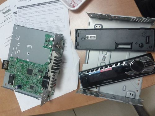
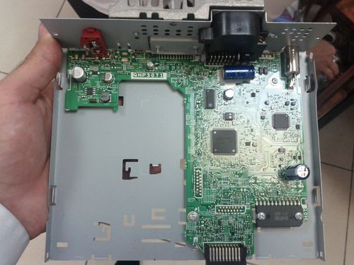
Бывает, что при движении на автомобиле выходит из строя автомагнитола, и тогда становится скучно в авто, особенно когда предстоит поездка одному и в дальнюю дорогу, например, в другой город. В этой статье попробуем разобраться в причинах выхода из строя автомагнитол и способах их устранения.
Кратко:
- 1 Ошибка усилителя магнитолы
- 2 Магнитола пишет «ошибка усилителя»
- 3 Почему выдается ошибка усилителя?
- 4 Магнитола перестает работать, не включается
- 5 Пропадает звук на автомагнитоле
- 6 Не читает cd или dvd диски
- 6.1 Сбивается воспроизведение диска при тряске
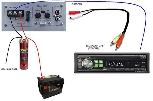
Ошибка усилителя магнитолы
Если с магнитолой творится что-то непонятное, может в колонках пропасть звук, через некоторое время опять начать работать, и так происходит на протяжении долгого времени, и при этом магнитола выдает ошибку усилителя, например такую: ERROR DC. В этом случае магнитола сообщает, что проблема с усилителем магнитолы.
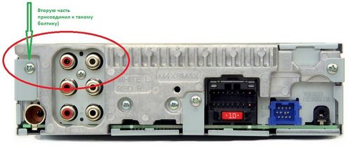
В этом случае требуется:
- Замерить напряжение на выходе усилителя;
- Подключить колонки к магнитоле в обход усилителя;
- Проверить разъемы в подключении на магнитоле (возможен плохой контакт);
- Проверить предохранители;
В случае если не помогли данные советы, тогда можно смело менять усилитель. Конечно, если есть время и лишние финансы, тогда можно найти электронщика и съездить к нему, может и поможет, разобрав усилитель, перепаяв схему и взяв денег, чуть меньше стоимости нового. Поэтому каждый делает свой выбор, как ему удобнее.
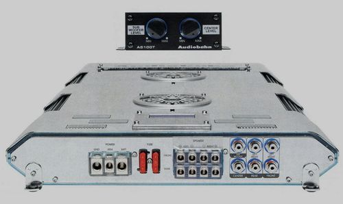
Магнитола пишет «ошибка усилителя»
Бывают магнитолы, такие как марки пионер, на которой так и отображается ошибка: «Ошибка усилителя». В этом случае можно провести все вышеописанные операции. И обязательно проверить все контакты. Если есть скрутки, то необходимо переделать на жесткое соединение, например, поставить колодку с болтовыми зажимами.
Если после приведенных выше «манипуляций» магнитола «вылечилась», тогда радуемся и наслаждаемся звучанием магнитолы. Но если никаких изменений не произошло, и ошибка усилителя магнитолы Пионер продолжает и дальше гореть на дисплее магнитолы, тогда необходимо профессиональное «лечение» – нужно нести автомагнитолу к специалистам в мастерскую, если дорога магнитола.
Почему выдается ошибка усилителя?
Теперь необходимо разобраться, в чем дело. Почему выдаются вышеописанные ошибки, и магнитолы выходят из строя?
По статистике, очень много автомобильных магнитол поступает на ремонт с одной проблемой – исчез звук у магнитолы. После выявления неисправности проблема выражается зачастую в выходе из строя усилителя звука автомагнитолы.
После диагностики магнитолы выявленная причина очень проста – сгорел усилитель автомагнитолы. Почему горят усилители?
Все мы любим при движении на автомобиле врубить музыку погромче, так чтобы уши закладывало. Вот это зачастую и является той причиной, по которой горят автомагнитолы. Это совершенно не значит, что музыку можно слушать только потихоньку. Это значит, что производитель, изначально экономя на запчастях, ставит в магнитолы заведомо некачественные микросхемы. В основном данная проблема происходит с автомагнитолами, которые являются не подлинной маркой производителя, а так называемые «копии», собранные в Китае.
Поэтому и проблема происходит такая только с некачественными магнитолами. Обладатели же оригинальных магнитол с такими проблемами не сталкиваются.
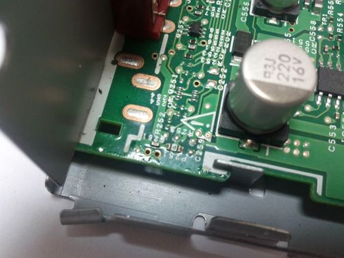
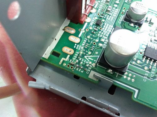
Еще одной из распространенных причин, когда магнитола Пионер пишет «ошибка усилителя», является короткое замыкание. Оно может случиться где угодно: в соединениях на магнитоле, на проводах, которые идут на колонки, на самых колонках. Возможно, провод производит короткое замыкание вследствие того, что он перебит чем-нибудь. Это как раз такой случай, когда необходимо проверить все соединения, а также провода в целом, но конечно будет лучше сразу съездить в автосервис, где на профессиональном оборудовании проведут диагностику и выявят короткое замыкание. И сразу произведут проверку усилителя автомагнитолы, потому что если в этом случае не погаснет ошибка усилителя магнитолы Pioneer, есть вероятность того, что усилитель просто-напросто сгорел.
Еще один способ устранить неисправность ошибки усилителя, но только для знающих и понимающих людей в электронике. Сам усилитель представляет собой микросхему с несколькими так называемыми ногами – металлическими штырьками. Так вот отрубаем первую из них, и все – сообщения нет, а автомагнитола работает исправно, но повторюсь, если не поняли, про что написано, лучше не лезть.
Далее немного подробнее остановимся на неисправностях автомагнитол.
Магнитола перестает работать, не включается
В этом случае необходимо проверить питание магнитолы, возможно, разрядился аккумулятор, неплотное прилегание разъемов питающего провода и магнитолы. Также возможно, что сгорел предохранитель в панели предохранителей автомобиля. Исправить можно, просто устранив все вышеперечисленные проблемы.
Пропадает звук на автомагнитоле
Необходимо проверить подключение колонок в разъемах выхода от магнитолы. Проверить целостность проводов. Рассмотреть все случаи, перечисленные в статье и описанные в разделе «Ошибки усилителя магнитолы».
Не читает cd или dvd диски
В том случае, когда не производит считывания дисков, это может быть проблема в головке считывания, которая либо вышла из строя, либо просто загрязнилась, и необходимо ее почистить. Для этих целей достаточно поставить чистящий диск, который и произведет чистку лазерной головки. Если проблема не устранилась, тогда следует сдать магнитолу на диагностику.
Сбивается воспроизведение диска при тряске
В данном случае есть вероятность того, что вышли из строя амортизаторы, расположенные в магнитоле, исправить возможно, только выполнив ремонт амортизаторов автомагнитолы.
Может случиться такая неисправность как невозможность загрузки или выгрузки диска. В этом случае стоит обратить внимание на мотор дисковода, при выходе которого может происходить такого рода неисправность. Стоит произвести ремонт или замену мотора самостоятельно, если понимаете в этом, или отремонтировать в мастерской.
В заключении данной статьи хотелось бы отметить тот факт, что при загрязнении автомагнитол появляется ряд неисправностей, поэтому держите свою магнитолу в чистоте!