«A2D» redirects here. For the U.S. Navy attack aircraft, see Douglas A2D Skyshark.

AD570 8-bit successive-approximation analog-to-digital converter

INTERSIL ICL7107. 31/2 digit single-chip A/D converter

In electronics, an analog-to-digital converter (ADC, A/D, or A-to-D) is a system that converts an analog signal, such as a sound picked up by a microphone or light entering a digital camera, into a digital signal. An ADC may also provide an isolated measurement such as an electronic device that converts an analog input voltage or current to a digital number representing the magnitude of the voltage or current. Typically the digital output is a two’s complement binary number that is proportional to the input, but there are other possibilities.
There are several ADC architectures. Due to the complexity and the need for precisely matched components, all but the most specialized ADCs are implemented as integrated circuits (ICs). These typically take the form of metal–oxide–semiconductor (MOS) mixed-signal integrated circuit chips that integrate both analog and digital circuits.
A digital-to-analog converter (DAC) performs the reverse function; it converts a digital signal into an analog signal.
Explanation[edit]
An ADC converts a continuous-time and continuous-amplitude analog signal to a discrete-time and discrete-amplitude digital signal. The conversion involves quantization of the input, so it necessarily introduces a small amount of error or noise. Furthermore, instead of continuously performing the conversion, an ADC does the conversion periodically, sampling the input, limiting the allowable bandwidth of the input signal.
The performance of an ADC is primarily characterized by its bandwidth and signal-to-noise ratio (SNR). The bandwidth of an ADC is characterized primarily by its sampling rate. The SNR of an ADC is influenced by many factors, including the resolution, linearity and accuracy (how well the quantization levels match the true analog signal), aliasing and jitter. The SNR of an ADC is often summarized in terms of its effective number of bits (ENOB), the number of bits of each measure it returns that are on average not noise. An ideal ADC has an ENOB equal to its resolution. ADCs are chosen to match the bandwidth and required SNR of the signal to be digitized. If an ADC operates at a sampling rate greater than twice the bandwidth of the signal, then per the Nyquist–Shannon sampling theorem, perfect reconstruction is possible. The presence of quantization error limits the SNR of even an ideal ADC. However, if the SNR of the ADC exceeds that of the input signal, its effects may be neglected resulting in an essentially perfect digital representation of the analog input signal.
Resolution[edit]

Fig. 1. An 8-level ADC coding scheme
The resolution of the converter indicates the number of different, ie discrete, values it can produce over the allowed range of analog input values. Thus a particular resolution determines the magnitude of the quantization error and therefore determines the maximum possible signal-to-noise ratio for an ideal ADC without the use of oversampling. The input samples are usually stored electronically in binary form within the ADC, so the resolution is usually expressed as the audio bit depth. In consequence, the number of discrete values available is usually a power of two. For example, an ADC with a resolution of 8 bits can encode an analog input to one in 256 different levels (28 = 256). The values can represent the ranges from 0 to 255 (i.e. as unsigned integers) or from −128 to 127 (i.e. as signed integer), depending on the application.
Resolution can also be defined electrically, and expressed in volts. The change in voltage required to guarantee a change in the output code level is called the least significant bit (LSB) voltage. The resolution Q of the ADC is equal to the LSB voltage. The voltage resolution of an ADC is equal to its overall voltage measurement range divided by the number of intervals:

where M is the ADC’s resolution in bits and EFSR is the full scale voltage range (also called ‘span’). EFSR is given by

where VRefHi and VRefLow are the upper and lower extremes, respectively, of the voltages that can be coded.
Normally, the number of voltage intervals is given by

where M is the ADC’s resolution in bits.[1]
That is, one voltage interval is assigned in between two consecutive code levels.
Example:
- Coding scheme as in figure 1
- Full scale measurement range = 0 to 1 volt
- ADC resolution is 3 bits: 23 = 8 quantization levels (codes)
- ADC voltage resolution, Q = 1 V / 8 = 0.125 V.
In many cases, the useful resolution of a converter is limited by the signal-to-noise ratio (SNR) and other errors in the overall system expressed as an ENOB.
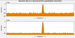
Comparison of quantizing a sinusoid to 64 levels (6 bits) and 256 levels (8 bits). The additive noise created by 6-bit quantization is 12 dB greater than the noise created by 8-bit quantization. When the spectral distribution is flat, as in this example, the 12 dB difference manifests as a measurable difference in the noise floors.
Quantization error[edit]

Analog to digital conversion as shown with fig. 1 and fig. 2.
Quantization error is introduced by the quantization inherent in an ideal ADC. It is a rounding error between the analog input voltage to the ADC and the output digitized value. The error is nonlinear and signal-dependent. In an ideal ADC, where the quantization error is uniformly distributed between −1/2 LSB and +1/2 LSB, and the signal has a uniform distribution covering all quantization levels, the signal-to-quantization-noise ratio (SQNR) is given by
 [2]
[2]

where Q is the number of quantization bits. For example, for a 16-bit ADC, the quantization error is 96.3 dB below the maximum level.
Quantization error is distributed from DC to the Nyquist frequency. Consequently, if part of the ADC’s bandwidth is not used, as is the case with oversampling, some of the quantization error will occur out-of-band, effectively improving the SQNR for the bandwidth in use. In an oversampled system, noise shaping can be used to further increase SQNR by forcing more quantization error out of band.
Dither[edit]
In ADCs, performance can usually be improved using dither. This is a very small amount of random noise (e.g. white noise), which is added to the input before conversion. Its effect is to randomize the state of the LSB based on the signal. Rather than the signal simply getting cut off altogether at low levels, it extends the effective range of signals that the ADC can convert, at the expense of a slight increase in noise. Note that dither can only increase the resolution of a sampler. It cannot improve the linearity, and thus accuracy does not necessarily improve.
Quantization distortion in an audio signal of very low level with respect to the bit depth of the ADC is correlated with the signal and sounds distorted and unpleasant. With dithering, the distortion is transformed into noise. The undistorted signal may be recovered accurately by averaging over time. Dithering is also used in integrating systems such as electricity meters. Since the values are added together, the dithering produces results that are more exact than the LSB of the analog-to-digital converter.
Dither is often applied when quantizing photographic images to a fewer number of bits per pixel—the image becomes noisier but to the eye looks far more realistic than the quantized image, which otherwise becomes banded. This analogous process may help to visualize the effect of dither on an analog audio signal that is converted to digital.
Accuracy[edit]
An ADC has several sources of errors. Quantization error and (assuming the ADC is intended to be linear) non-linearity are intrinsic to any analog-to-digital conversion. These errors are measured in a unit called the least significant bit (LSB). In the above example of an eight-bit ADC, an error of one LSB is 1/256 of the full signal range, or about 0.4%.
Nonlinearity[edit]
All ADCs suffer from nonlinearity errors caused by their physical imperfections, causing their output to deviate from a linear function (or some other function, in the case of a deliberately nonlinear ADC) of their input. These errors can sometimes be mitigated by calibration, or prevented by testing. Important parameters for linearity are integral nonlinearity and differential nonlinearity. These nonlinearities introduce distortion that can reduce the signal-to-noise ratio performance of the ADC and thus reduce its effective resolution.
Jitter[edit]
When digitizing a sine wave  , the use of a non-ideal sampling clock will result in some uncertainty in when samples are recorded. Provided that the actual sampling time uncertainty due to clock jitter is
  , the error caused by this phenomenon can be estimated as
  . This will result in additional recorded noise that will reduce the effective number of bits (ENOB) below that predicted by quantization error alone. The error is zero for DC, small at low frequencies, but significant with signals of high amplitude and high frequency. The effect of jitter on performance can be compared to quantization error:
  , where q is the number of ADC bits.[citation needed]
| Output size (bits) |
Signal Frequency | ||||||
|---|---|---|---|---|---|---|---|
| 1 Hz | 1 kHz | 10 kHz | 1 MHz | 10 MHz | 100 MHz | 1 GHz | |
| 8 | 1,243 µs | 1.24 µs | 124 ns | 1.24 ns | 124 ps | 12.4 ps | 1.24 ps |
| 10 | 311 µs | 311 ns | 31.1 ns | 311 ps | 31.1 ps | 3.11 ps | 0.31 ps |
| 12 | 77.7 µs | 77.7 ns | 7.77 ns | 77.7 ps | 7.77 ps | 0.78 ps | 0.08 ps («77.7fs») |
| 14 | 19.4 µs | 19.4 ns | 1.94 ns | 19.4 ps | 1.94 ps | 0.19 ps | 0.02 ps («19.4fs») |
| 16 | 4.86 µs | 4.86 ns | 486 ps | 4.86 ps | 0.49 ps | 0.05 ps («48.5 fs») | – |
| 18 | 1.21 µs | 1.21 ns | 121 ps | 1.21 ps | 0.12 ps | – | – |
| 20 | 304 ns | 304 ps | 30.4 ps | 0.30 ps («303.56 fs») | 0.03 ps («30.3 fs») | – | – |
| 24 | 18.9 ns | 18.9 ps | 1.89 ps | 0.019 ps («18.9 fs») | — | – | – |
Clock jitter is caused by phase noise.[3][4] The resolution of ADCs with a digitization bandwidth between 1 MHz and 1 GHz is limited by jitter.[5] For lower bandwidth conversions such as when sampling audio signals at 44.1 kHz, clock jitter has a less significant impact on performance.[6]
Sampling rate[edit]
An analog signal is continuous in time and it is necessary to convert this to a flow of digital values. It is therefore required to define the rate at which new digital values are sampled from the analog signal. The rate of new values is called the sampling rate or sampling frequency of the converter. A continuously varying bandlimited signal can be sampled and then the original signal can be reproduced from the discrete-time values by a reconstruction filter. The Nyquist–Shannon sampling theorem implies that a faithful reproduction of the original signal is only possible if the sampling rate is higher than twice the highest frequency of the signal.
Since a practical ADC cannot make an instantaneous conversion, the input value must necessarily be held constant during the time that the converter performs a conversion (called the conversion time). An input circuit called a sample and hold performs this task—in most cases by using a capacitor to store the analog voltage at the input, and using an electronic switch or gate to disconnect the capacitor from the input. Many ADC integrated circuits include the sample and hold subsystem internally.
Aliasing[edit]
An ADC works by sampling the value of the input at discrete intervals in time. Provided that the input is sampled above the Nyquist rate, defined as twice the highest frequency of interest, then all frequencies in the signal can be reconstructed. If frequencies above half the Nyquist rate are sampled, they are incorrectly detected as lower frequencies, a process referred to as aliasing. Aliasing occurs because instantaneously sampling a function at two or fewer times per cycle results in missed cycles, and therefore the appearance of an incorrectly lower frequency. For example, a 2 kHz sine wave being sampled at 1.5 kHz would be reconstructed as a 500 Hz sine wave.
To avoid aliasing, the input to an ADC must be low-pass filtered to remove frequencies above half the sampling rate. This filter is called an anti-aliasing filter, and is essential for a practical ADC system that is applied to analog signals with higher frequency content. In applications where protection against aliasing is essential, oversampling may be used to greatly reduce or even eliminate it.
Although aliasing in most systems is unwanted, it can be exploited to provide simultaneous down-mixing of a band-limited high-frequency signal (see undersampling and frequency mixer). The alias is effectively the lower heterodyne of the signal frequency and sampling frequency.[7]
Oversampling[edit]
For economy, signals are often sampled at the minimum rate required with the result that the quantization error introduced is white noise spread over the whole passband of the converter. If a signal is sampled at a rate much higher than the Nyquist rate and then digitally filtered to limit it to the signal bandwidth produces the following advantages:
- Oversampling can make it easier to realize analog anti-aliasing filters
- Improved audio bit depth
- Reduced noise, especially when noise shaping is employed in addition to oversampling.
Oversampling is typically used in audio frequency ADCs where the required sampling rate (typically 44.1 or 48 kHz) is very low compared to the clock speed of typical transistor circuits (>1 MHz). In this case, the performance of the ADC can be greatly increased at little or no cost. Furthermore, as any aliased signals are also typically out of band, aliasing can often be completely eliminated using very low cost filters.
Relative speed and precision[edit]
The speed of an ADC varies by type. The Wilkinson ADC is limited by the clock rate which is processable by current digital circuits. For a successive-approximation ADC, the conversion time scales with the logarithm of the resolution, i.e. the number of bits. Flash ADCs are certainly the fastest type of the three; The conversion is basically performed in a single parallel step.
There is a potential tradeoff between speed and precision. Flash ADCs have drifts and uncertainties associated with the comparator levels results in poor linearity. To a lesser extent, poor linearity can also be an issue for successive-approximation ADCs. Here, nonlinearity arises from accumulating errors from the subtraction processes. Wilkinson ADCs have the best linearity of the three.[8][9]
Sliding scale principle[edit]
The sliding scale or randomizing method can be employed to greatly improve the linearity of any type of ADC, but especially flash and successive approximation types. For any ADC the mapping from input voltage to digital output value is not exactly a floor or ceiling function as it should be. Under normal conditions, a pulse of a particular amplitude is always converted to the same digital value. The problem lies in that the ranges of analog values for the digitized values are not all of the same widths, and the differential linearity decreases proportionally with the divergence from the average width. The sliding scale principle uses an averaging effect to overcome this phenomenon. A random, but known analog voltage is added to the sampled input voltage. It is then converted to digital form, and the equivalent digital amount is subtracted, thus restoring it to its original value. The advantage is that the conversion has taken place at a random point. The statistical distribution of the final levels is decided by a weighted average over a region of the range of the ADC. This in turn desensitizes it to the width of any specific level.[10][11]
Types[edit]
These are several common ways of implementing an electronic ADC.
Direct-conversion[edit]
A direct-conversion or flash ADC has a bank of comparators sampling the input signal in parallel, each firing for a specific voltage range. The comparator bank feeds a digital encoder[disambiguation needed] logic circuit that generates a binary number on the output lines for each voltage range.
ADCs of this type have a large die size and high power dissipation. They are often used for video, wideband communications, or other fast signals in optical and magnetic storage.
The circuit consists of a resistive divider network, a set of op-amp comparators and a priority encoder. A small amount of hysteresis is built into the comparator to resolve any problems at voltage boundaries. At each node of the resistive divider, a comparison voltage is available. The purpose of the circuit is to compare the analog input voltage with each of the node voltages.
The circuit has the advantage of high speed as the conversion takes place simultaneously rather than sequentially. Typical conversion time is 100 ns or less. Conversion time is limited only by the speed of the comparator and of the priority encoder. This type of ADC has the disadvantage that the number of comparators required almost doubles for each added bit. Also, the larger the value of n, the more complex is the priority encoder.
Successive approximation[edit]
A successive-approximation ADC uses a comparator and a binary search to successively narrow a range that contains the input voltage. At each successive step, the converter compares the input voltage to the output of an internal digital-to-analog converter (DAC) which initially represents the midpoint of the allowed input voltage range. At each step in this process, the approximation is stored in a successive approximation register (SAR) and the output of the digital-to-analog converter is updated for a comparison over a narrower range.
Ramp-compare[edit]
A ramp-compare ADC produces a saw-tooth signal that ramps up or down then quickly returns to zero.[12]
When the ramp starts, a timer starts counting. When the ramp voltage matches the input, a comparator fires, and the timer’s value is recorded. Timed ramp converters can be implemented economically,[a] however, the ramp time may be sensitive to temperature because the circuit generating the ramp is often a simple analog integrator. A more accurate converter uses a clocked counter driving a DAC. A special advantage of the ramp-compare system is that converting a second signal just requires another comparator and another register to store the timer value. To reduce sensitivity to input changes during conversion, a sample and hold can charge a capacitor with the instantaneous input voltage and the converter can time the time required to discharge with a constant current.
Wilkinson[edit]
The Wilkinson ADC was designed by Denys Wilkinson in 1950. The Wilkinson ADC is based on the comparison of an input voltage with that produced by a charging capacitor. The capacitor is allowed to charge until a comparator determines it matches the input voltage. Then, the capacitor is discharged linearly. The time required to discharge the capacitor is proportional to the amplitude of the input voltage. While the capacitor is discharging, pulses from a high-frequency oscillator clock are counted by a register. The number of clock pulses recorded in the register is also proportional to the input voltage.[14][15]
Integrating[edit]
An integrating ADC (also dual-slope or multi-slope ADC) applies the unknown input voltage to the input of an integrator and allows the voltage to ramp for a fixed time period (the run-up period). Then a known reference voltage of opposite polarity is applied to the integrator and is allowed to ramp until the integrator output returns to zero (the run-down period). The input voltage is computed as a function of the reference voltage, the constant run-up time period, and the measured run-down time period. The run-down time measurement is usually made in units of the converter’s clock, so longer integration times allow for higher resolutions. Likewise, the speed of the converter can be improved by sacrificing resolution. Converters of this type (or variations on the concept) are used in most digital voltmeters for their linearity and flexibility.
- Charge balancing ADC
- The principle of charge balancing ADC is to first convert the input signal to a frequency using a voltage-to-frequency converter. This frequency is then measured by a counter and converted to an output code proportional to the analog input. The main advantage of these converters is that it is possible to transmit frequency even in a noisy environment or in isolated form. However, the limitation of this circuit is that the output of the voltage-to-frequency converter depends upon an RC product whose value cannot be accurately maintained over temperature and time.
- Dual-slope ADC
- The analog part of the circuit consists of a high input impedance buffer, precision integrator and a voltage comparator. The converter first integrates the analog input signal for a fixed duration and then it integrates an internal reference voltage of opposite polarity until the integrator output is zero. The main disadvantage of this circuit is the long duration time. They are particularly suitable for accurate measurement of slowly varying signals such as thermocouples and weighing scales.
Delta-encoded[edit]
A delta-encoded or counter-ramp ADC has an up-down counter that feeds a DAC. The input signal and the DAC both go to a comparator. The comparator controls the counter. The circuit uses negative feedback from the comparator to adjust the counter until the DAC’s output matches the input signal and number is read from the counter. Delta converters have very wide ranges and high resolution, but the conversion time is dependent on the input signal behavior, though it will always have a guaranteed worst-case. Delta converters are often very good choices to read real-world signals as most signals from physical systems do not change abruptly. Some converters combine the delta and successive approximation approaches; this works especially well when high frequency components of the input signal are known to be small in magnitude.
Pipelined[edit]
A pipelined ADC (also called subranging quantizer) uses two or more conversion steps. First, a coarse conversion is done. In a second step, the difference to the input signal is determined with a DAC. This difference is then converted more precisely, and the results are combined in the last step. This can be considered a refinement of the successive-approximation ADC wherein the feedback reference signal consists of the interim conversion of a whole range of bits (for example, four bits) rather than just the next-most-significant bit. By combining the merits of the successive approximation and flash ADCs this type is fast, has a high resolution, and can be implemented efficiently.
Sigma-delta[edit]
A sigma-delta ADC (also known as a delta-sigma ADC) is based on a feedback loop with an analog filter and low resolution (often 1 bit), but high speed ADC and DAC to approximate the incoming signal. The filter (usually a 2nd order low pass filter) in the loop performs noise shaping: the quantization noise originating from the DAC is no longer evenly distributed over the frequencies, but higher for the high frequencies and reduced for the low frequencies.
A digital filter (decimation filter) than removes much of the higher frequencies (especially much of the quantization noise) and converts the data stream from high sampling rate and low resolution to low speed and high resolution.
Time-interleaved[edit]
A time-interleaved ADC uses M parallel ADCs where each ADC samples data every M:th cycle of the effective sample clock. The result is that the sample rate is increased M times compared to what each individual ADC can manage. In practice, the individual differences between the M ADCs degrade the overall performance reducing the spurious-free dynamic range (SFDR).[16] However, techniques exist to correct for these time-interleaving mismatch errors.[17]
Intermediate FM stage[edit]
An ADC with an intermediate FM stage first uses a voltage-to-frequency converter to produce an oscillating signal with a frequency proportional to the voltage of the input signal, and then uses a frequency counter to convert that frequency into a digital count proportional to the desired signal voltage. Longer integration times allow for higher resolutions. Likewise, the speed of the converter can be improved by sacrificing resolution. The two parts of the ADC may be widely separated, with the frequency signal passed through an opto-isolator or transmitted wirelessly. Some such ADCs use sine wave or square wave frequency modulation; others use pulse-frequency modulation. Such ADCs were once the most popular way to show a digital display of the status of a remote analog sensor.[18][19][20][21][22]
Time-stretch[edit]
A Time-stretch analog-to-digital converter (TS-ADC) digitizes a very wide bandwidth analog signal, that cannot be digitized by a conventional electronic ADC, by time-stretching the signal prior to digitization. It commonly uses a photonic preprocessor to time-stretch the signal, which effectively slows the signal down in time and compresses its bandwidth. As a result, an electronic ADC, that would have been too slow to capture the original signal, can now capture this slowed-down signal. For continuous capture of the signal, the frontend also divides the signal into multiple segments in addition to time-stretching. Each segment is individually digitized by a separate electronic ADC. Finally, a digital signal processor rearranges the samples and removes any distortions added by the preprocessor to yield the binary data that is the digital representation of the original analog signal.
Commercial[edit]
In many cases, the most expensive part of an integrated circuit is the pins, because they make the package larger, and each pin has to be connected to the integrated circuit’s silicon. To save pins, it is common for ADCs to send their data one bit at a time over a serial interface to the computer, with each bit coming out when a clock signal changes state. This saves quite a few pins on the ADC package, and in many cases, does not make the overall design any more complex.
Commercial ADCs often have several inputs that feed the same converter, usually through an analog multiplexer. Different models of ADC may include sample and hold circuits, instrumentation amplifiers or differential inputs, where the quantity measured is the difference between two inputs.
Applications[edit]
Music recording[edit]
Analog-to-digital converters are integral to modern music reproduction technology and digital audio workstation-based sound recording. Music may be produced on computers using an analog recording and therefore analog-to-digital converters are needed to create the pulse-code modulation (PCM) data streams that go onto compact discs and digital music files. The current crop of analog-to-digital converters utilized in music can sample at rates up to 192 kilohertz. Many recording studios record in 24-bit/96 kHz pulse-code modulation (PCM) format and then downsample and dither the signal for Compact Disc Digital Audio production (44.1 kHz) or to 48 kHz for radio and television broadcast applications.
Digital signal processing[edit]
ADCs are required in digital signal processing systems that process, store, or transport virtually any analog signal in digital form. TV tuner cards, for example, use fast video analog-to-digital converters. Slow on-chip 8-, 10-, 12-, or 16-bit analog-to-digital converters are common in microcontrollers. Digital storage oscilloscopes need very fast analog-to-digital converters, also crucial for software-defined radio and their new applications.
Scientific instruments[edit]
Digital imaging systems commonly use analog-to-digital converters for digitizing pixels. Some radar systems use analog-to-digital converters to convert signal strength to digital values for subsequent signal processing. Many other in situ and remote sensing systems commonly use analogous technology.
Many sensors in scientific instruments produce an analog signal; temperature, pressure, pH, light intensity etc. All these signals can be amplified and fed to an ADC to produce a digital representation.
Rotary encoder[edit]
Some non-electronic or only partially electronic devices, such as rotary encoders, can also be considered ADCs. Typically the digital output of an ADC will be a two’s complement binary number that is proportional to the input. An encoder might output a Gray code.
Displays[edit]
Flat-panel displays are inherently digital and need an ADC to process an analog signal such as composite or VGA.
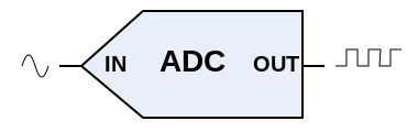
Electrical symbol[edit]
Testing[edit]
Testing an analog-to-digital converter requires an analog input source and hardware to send control signals and capture digital data output. Some ADCs also require an accurate source of reference signal.
The key parameters to test an ADC are:
- DC offset error
- DC gain error
- signal-to-noise ratio (SNR)
- Total harmonic distortion (THD)
- Integral nonlinearity (INL)
- Differential nonlinearity (DNL)
- Spurious free dynamic range
- Power dissipation
See also[edit]
- Adaptive predictive coding, a type of ADC in which the value of the signal is predicted by a linear function
- Audio codec
- Beta encoder
- Integral linearity
- Modem
Notes[edit]
- ^ A very simple (nonlinear) ramp converter can be implemented with a microcontroller and one resistor and capacitor.[13]
References[edit]
- ^ «Principles of Data Acquisition and Conversion» (PDF). Texas Instruments. April 2015. Archived (PDF) from the original on October 9, 2022. Retrieved October 18, 2016.
- ^ Lathi, B.P. (1998). Modern Digital and Analog Communication Systems (3rd ed.). Oxford University Press.
- ^ «Maxim App 800: Design a Low-Jitter Clock for High-Speed Data Converters», maxim-ic.com, July 17, 2002
- ^ «Jitter effects on Analog to Digital and Digital to Analog Converters» (PDF). Retrieved August 19, 2012.
- ^ Löhning, Michael; Fettweis, Gerhard (2007). «The effects of aperture jitter and clock jitter in wideband ADCs». Computer Standards & Interfaces Archive. 29 (1): 11–18. CiteSeerX 10.1.1.3.9217. doi:10.1016/j.csi.2005.12.005.
- ^ Redmayne, Derek; Steer, Alison (December 8, 2008), «Understanding the effect of clock jitter on high-speed ADCs», eetimes.com
- ^ «RF-Sampling and GSPS ADCs – Breakthrough ADCs Revolutionize Radio Architectures» (PDF). Texas Instruments. Archived (PDF) from the original on October 9, 2022. Retrieved November 4, 2013.
- ^ Knoll (1989, pp. 664–665)
- ^ Nicholson (1974, pp. 313–315)
- ^ Knoll (1989, pp. 665–666)
- ^ Nicholson (1974, pp. 315–316)
- ^ Couch — 2001 — Digital and analog communication systems — Prentice Hall — New Jersey, USA
- ^ «Atmel Application Note AVR400: Low Cost A/D Converter» (PDF). atmel.com. Archived (PDF) from the original on October 9, 2022.
- ^ Knoll (1989, pp. 663–664)
- ^ Nicholson (1974, pp. 309–310)
- ^ Vogel, Christian (2005). «The Impact of Combined Channel Mismatch Effects in Time-interleaved ADCs». IEEE Transactions on Instrumentation and Measurement. 55 (1): 415–427. CiteSeerX 10.1.1.212.7539. doi:10.1109/TIM.2004.834046. S2CID 15038020.
- ^ Gabriele Manganaro; David H. Robertson (July 2015), Interleaving ADCs: Unraveling the Mysteries, Analog Devices, retrieved October 7, 2021
- ^
Analog Devices MT-028 Tutorial: «Voltage-to-Frequency Converters» by Walt Kester and James Bryant 2009,
apparently adapted from Kester, Walter Allan (2005) Data conversion handbook, Newnes, p. 274, ISBN 0750678410. - ^
Microchip AN795 «Voltage to Frequency / Frequency to Voltage Converter» p. 4: «13-bit A/D converter» - ^ Carr, Joseph J. (1996) Elements of electronic instrumentation and measurement, Prentice Hall, p. 402, ISBN 0133416860.
- ^ «Voltage-to-Frequency Analog-to-Digital Converters». globalspec.com
- ^ Pease, Robert A. (1991) Troubleshooting Analog Circuits, Newnes, p. 130, ISBN 0750694998.
- Knoll, Glenn F. (1989). Radiation Detection and Measurement (2nd ed.). New York: John Wiley & Sons. ISBN 978-0471815044.
- Nicholson, P. W. (1974). Nuclear Electronics. New York: John Wiley & Sons. pp. 315–316. ISBN 978-0471636977.
Further reading[edit]
- Allen, Phillip E.; Holberg, Douglas R. (2002). CMOS Analog Circuit Design. ISBN 978-0-19-511644-1.
- Fraden, Jacob (2010). Handbook of Modern Sensors: Physics, Designs, and Applications. Springer. ISBN 978-1441964656.
- Kester, Walt, ed. (2005). The Data Conversion Handbook. Elsevier: Newnes. ISBN 978-0-7506-7841-4.
- Johns, David; Martin, Ken (1997). Analog Integrated Circuit Design. ISBN 978-0-471-14448-9.
- Liu, Mingliang (2006). Demystifying Switched-Capacitor Circuits. ISBN 978-0-7506-7907-7.
- Norsworthy, Steven R.; Schreier, Richard; Temes, Gabor C. (1997). Delta-Sigma Data Converters. IEEE Press. ISBN 978-0-7803-1045-2.
- Razavi, Behzad (1995). Principles of Data Conversion System Design. New York, NY: IEEE Press. ISBN 978-0-7803-1093-3.
- Ndjountche, Tertulien (May 24, 2011). CMOS Analog Integrated Circuits: High-Speed and Power-Efficient Design. Boca Raton, FL: CRC Press. ISBN 978-1-4398-5491-4.
- Staller, Len (February 24, 2005). «Understanding analog to digital converter specifications». Embedded Systems Design.
- Walden, R. H. (1999). «Analog-to-digital converter survey and analysis». IEEE Journal on Selected Areas in Communications. 17 (4): 539–550. CiteSeerX 10.1.1.352.1881. doi:10.1109/49.761034.
External links[edit]
- An Introduction to Delta Sigma Converters A very nice overview of Delta-Sigma converter theory.
- Digital Dynamic Analysis of A/D Conversion Systems through Evaluation Software based on FFT/DFT Analysis RF Expo East, 1987
- Which ADC Architecture Is Right for Your Application? article by Walt Kester
- ADC and DAC Glossary at the Wayback Machine (archived 2009-11-24) Defines commonly used technical terms
- Introduction to ADC in AVR – Analog to digital conversion with Atmel microcontrollers
- Signal processing and system aspects of time-interleaved ADCs
- MATLAB Simulink model of a simple ramp ADC
Main Content
Most RF receivers in modern communications or radar systems feed signals to an analog-to-digital converter (ADC). Due to their finite resolution, ADCs introduce quantization error into the system. The resolution of the ADC is determined by the number of bits and the full-scale (FS) range of the ADC.
The preceding figure illustrates an RF signal that falls within the dynamic range (DR) of an ADC. The input signal and noise at the carrier fRF has high signal-to-noise ratio (SNR). The received signal at fIF has reduced SNR due to system noise figure. However, if the quantization error is near or above the receiver noise, system performance degrades.

To ensure that the ADC contributes no more than 0.1 dB of noise to the signal at fIF , the quantization noise floor must be 16 dB lower than the receiver noise. This condition can be met by:
-
Reducing the full-scale (FS) range or increasing the resolution of the ADC, which lowers the quantization noise floor.
-
Increasing the gain of the RF receiver, which raises the receiver noise floor.
Overcome Quantization Error of an ADC
The model ex_simrf_adc_rx simulates a low IF receiver with an ADC. This model is based on low IF receiver design from the Model System Noise Figure. At the output of the RF system, the ADC subsystem models an ADC with an FS range of sqrt(100e-3) V and a resolution of 16 bits.
open_system("ex_simrf_adc_rx")

The power of a voltage signal at the full-scale range of the ADC in dBm is
P_vs = 10*log10(sqrt(100^-3))+30 = 0
View Simulation Output
The power levels shown in the figures represent the power spectral density (PSD) of the signals in dBm/Hz.
The Spectrum Analyzer Block shows the power spectrum of the two-tone signal and noise at the input of the receiver-ADC system. The measured power of each tone of -142 dBm is consistent with the expected power level of a 0.1 uV signal. The power level of the noise is consistent with a -174 dBm/Hz noise floor. The output spectrum plot shows power spectrum of the output signal.


The quantization error exceeds the receiver noise.
Measure Quantization Noise Floor
To calculate the quantization noise floor (QNF_ADC) of the ADC, subtract the dynamic range from the full-scale power, which is 0 dBm. QNF_ADC is calculated using this equation:
QNF_ADC = 6.02*N_bits + 10*log10(deltaf) + 1.76 = 116.1 dBm/Hz
where
-
N_bits is the resolution. The ADC in this example uses 16 bits.
-
deltaf is the bandwidth of the FFT, which is 64 in this example. Oversampling in an ADC yields lower quantization noise.
-
The value 1.76 is a correction factor for a pure sinusoidal input.
Therefore, the quantization noise floor is -116 dBm/Hz, in agreement with the measured output levels.
Improving Receiver-ADC Performance
Increasing the gain in the mixer raises the receiver noise without increasing the noise figure. Calculate the mixer gain required to achieve a 16-dB margin between the quantization noise floor and the receiver noise:
G_mixer = (QNF_ADC+16) — (-174+G_sys+NF_sys) = (-116.1+16) — (-174+40+10) = 23.9 dB
To simulate a receiver that clears the quantization noise floor: set the Available power gain parameter of the mixer to 23.9 and click Run.
sim("ex_simrf_adc_rx_mixer")

The figure shows that the receiver noise is 16 dB above the quantization noise floor.
See Also
Mixer | Amplifier
Related Topics
- RF Noise Modeling
- Noise in RF Systems
Template:Unreferenced
The difference between the actual analog value and quantized digital value due is called quantization error. This error is due either to rounding or truncation.
Many physical quantities are actually quantized by physical entities. Examples of fields where this limitation applies include electronics (due to electrons), optics (due to photons), biology (due to DNA), and chemistry (due to molecules). This is sometimes known as the «quantum noise limit» of systems in those fields. This is a different manifestation of «quantization error,» in which theoretical models may be analog but physics occurs digitally. Around the quantum limit, the distinction between analog and digital quantities vanishes.
Quantization noise model of quantization error[]
File:Quanterr.png Quantization noise. The difference between the blue and red signals in the upper graph is the quantization error, which is «added» to the original signal and is the source of noise.
Quantization noise is a model of quantization error introduced by quantization in the analog-to-digital conversion (ADC) process in telecommunication systems and signal processing. It is a rounding error between the analogue input voltage to the ADC and the output digitized value. The noise is non-linear and signal-dependent. It can be modelled in several different ways.
In an ideal analog-to-digital converter, where the quantization error is uniformly distributed between −1/2 LSB and +1/2 LSB, and the signal has a uniform distribution covering all quantization levels, the signal-to-noise ratio (SNR) can be calculated from

The most common test signals that fulfil this are full amplitude triangle waves and sawtooth waves.
In this case a 16-bit ADC has a maximum signal-to-noise ratio of 6.0206 · 16=96.33 dB.
When the input signal is a full-amplitude sine wave the distribution of the signal is no longer uniform, and the corresponding equation is instead

Here, the quantization noise is once again assumed to be uniformly distributed. When the input signal has a high amplitude and a wide frequency spectrum this is the case.[1]
In this case a 16-bit ADC has a maximum signal-to-noise ratio of 98.09 dB.
For complex signals in high-resolution ADCs this is an accurate model. For low-resolution ADCs, low-level signals in high-resolution ADCs, and for simple waveforms the quantization noise is not uniformly distributed, making this model inaccurate.[2] In these cases the quantization noise distribution is strongly affected by the exact amplitude of the signal.
Template:Listen
References[]
- ↑ Template:Cite book
- ↑ Template:Cite book
See also[]
- Round-off error
- Dither
- Analog to digital converter
- Quantization
- Quantization noise
- Discretization error
- Signal-to-noise ratio
- Bit resolution
- SQNR
External links[]
- Quantization noise in Digital Computation, Signal Processing, and Control, Bernard Widrow and István Kollár, 2007.
- The Relationship of Dynamic Range to Data Word Size in Digital Audio Processing
- Round-Off Error Variance — derivation of noise power of q²/12 for round-off error
- Dynamic Evaluation of High-Speed, High Resolution D/A Converters Outlines HD, IMD and NPR measurements, also includes a derivation of quantization noise
- Signal to quantization noise in quantized sinusoidal
de:Quantisierungsrauschen
es:Ruido de cuantificación
ja:量子化雑音
ja:量子化誤差
pl:Szum kwantyzacji
ru:Шум квантования
Analog To Digital Converter | How ADC Works And Reading Analog Signals
| Previous Tutorial | Tutorial 22 | Next Tutorial | ||
| Embedded Systems Tutorials With PIC MCUs | ||||
| Intermediate Level ★★☆☆☆ |
In this tutorial, you’ll get a solid introduction to the analog signal conversion to the digital domain. And why it’s important to do so. And how does ADC work in order to achieve such a goal? And what are the fundamental limitations and challenges for practical ADC? We’ll also see different schemes for how to read an ADC with an 8-Bit Microcontroller from Microchip (PIC). By the end of this long tutorial, you’ll understand the fundamental foundations of ADC and you’ll also create the 2 projects below from scratch. And have your own device driver for ADC for any future project you wanna create. Stick with me it’s gonna be so long, hopefully, informative journey! And let’s get started!
Tutorial Contents
- 1 Required Components
- 2 What is Analog To Digital Conversion?
- 3 Why We Need Analog To Digital Converters?
- 4 How ADC Works?
- 4.1 General Block Diagram For ADC
- 4.2 Analog Reference For ADC
- 4.3 ADC Sampling
- 4.3.1 Sampling Rate
- 4.3.2 Sampling Theorem
- 4.3.3 Over-Sampling
- 4.4 ADC Resolution & Quantization
- 4.4.1 Resolution
- 4.4.2 Quantization
- 4.4.3 Quantization Error
- 5 Different Types of ADC
- 5.1 Counter Type ADC
- 5.2 Integrating (Dual-Slope) ADC
- 5.3 Successive Approximation
- 5.4 Flash Type ADC (Direct)
- 6 ADC Module in PIC Microcontroller
- 6.1 Hardware Description
- 6.2 Block Diagram
- 6.3 ADC Special Function Registers
- 6.3.1 ADCON0 Register
- 6.3.2 ADCON1
- 6.4 Analog Reference
- 6.5 Channel Selection
- 6.6 A/D Aquisition Time
- 6.7 A/D Conversion Clock Selection
- 6.8 Starting A/D Conversion
- 6.9 A/D Conversion Sequence Timing
- 6.10 A/D Conversion Result Registers
- 6.11 Maximum Sampling Rate
- 7 Configuring ADC With PIC MCU
- 7.1 Steps To Configure The ADC Module
- 7.2 Implementing Simple ADC Driver
- 8 LED Dimmer – ADC LAB1
- 8.1 1. Coding
- 8.2 2. Simulation
- 8.3 3. Prototyping
- 9 Finger Snap Switch – ADC LAB2
- 9.1 1. Coding
- 9.2 2. Prototyping
- 10 Different Schemes To Read ADC
- 10.1 Single Channel Conversion
- 10.1.1 1 One Shot
- 10.1.2 2 Continuous Mode
- 10.2 Multiple Channels Conversion
- 10.2.1 1 Burst of Conversions
- 10.2.2 2 Continuous Bursts
- 10.1 Single Channel Conversion
- 11 Concluding Remarks
- 12 Share this:
- 13 Related
Required Components
| Qty. | Component Name | Buy On Amazon.com |
| 1 | PIC16F877A | Add |
| 1 | BreadBoard | Add |
| 1 | Potentiometer | Add Add |
| 1 | LED | Add Add |
| 1 | Microphone | Add Add |
| 1 | BC337 NPN BJT Transistor | Add Add |
| 1 | Resistors Kit (to build audio amp.) | Add Add |
| 1 | Capacitors Kit (to build audio amp.) | Add Add |
| 1 | USB-TTL (FTDI) Serial Converter | Add |
| 1 | Jumper Wires Pack | Add Add |
| 1 | LM7805 Voltage Regulator (5v) | Add |
| 1 | Crystal Oscillator | Add |
| 1 | PICkit2 or 3 Programmer | Add |
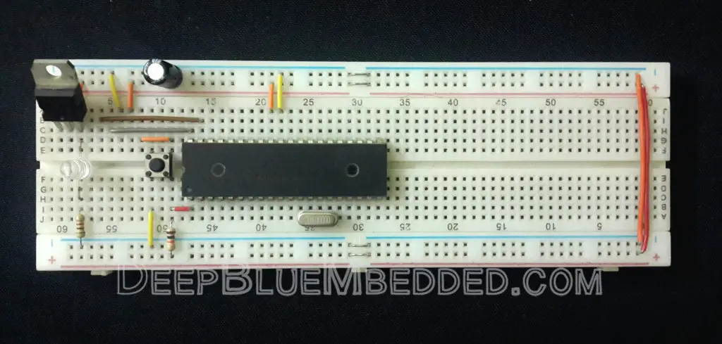
The Prototyping Board Setup
What is Analog To Digital Conversion?
It’s a process of capturing the analog electric signal (such as sound captured by a microphone) and converting it to a series of numeric “Digital” values to be stored/processed by a digital computer or DSP. The electronic device which is used for this conversion process has been known to be the A/D or ADC (Analog-To-Digital Converter).
There are many different types of A/D converters out there. And depending on how it works and how well it gets the job done, you pay more or less respectively per ADC unit.
And before any further investigation for ADC types and technical details of working principles, let us question about the usefulness of A/D conversion. Why do we need to use ADC in the first place?
Why We Need Analog To Digital Converters?
Our need to convert analog signals to digital data stems from the fact that our computers are digital ones. They just can’t handle the analog signal and therefore, there should be a device which converts the signal from analog to digital domain (ADC).
Most signals are analog in nature and the electronic sensors which we’re using for capturing these phenomena are also analog. For example, the temperature sensor converts temperature in °C to an analog voltage that’s proportional to the value of temperature. So do the microphone, pressure sensor, light sensor and so on.
Hence, we need a way to read analog voltage and convert it to digital values which we can program our computers to manipulate it mathematically in order to achieve real-time monitoring and/or control or whatever.
Image Credit to Ti.com
How ADC Works?
General Block Diagram For ADC
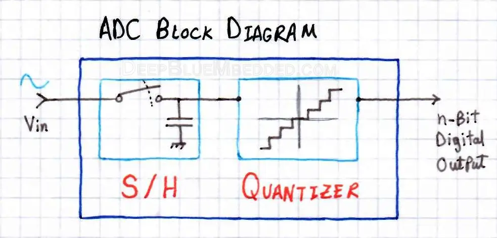
The basic structure of an ADC consists of an S/H circuit (Sample & Hold). Followed by a quantized which is actually the working horse for the analog to the digital conversion process. The type of ADC depends on how it’s performing the quantization process, it can be analog integration, digital counter, successive approximation, or even direct conversion as in Flash ADC types which we’ll discuss hereafter.
Finally, the digital output data is served to the CPU or gets directly stored in memory. The ADC can either be integrated within the MCU chip itself or a standalone IC that you can interface with Serial/Parallel ports of your microcontroller.
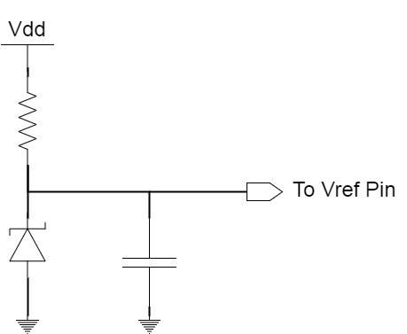
Analog Reference For ADC
Analog To Digital Conversion process needs an extremely stable voltage reference Vref+ and Vref– representing the maximum allowable voltage swing for the input in order to be correctly converted to digital value with respect to the limits which are set by the analog reference Vref.
The easiest way to guarantee a stable Vref is to use a resistor and a capacitor to resist any sudden drop in voltage and protect your system. You can also use a Zener diode as well to guarantee a stable voltage reference which immunes your system against any sudden changes in power supply increase/drop. The concept is indicated in the diagram below.
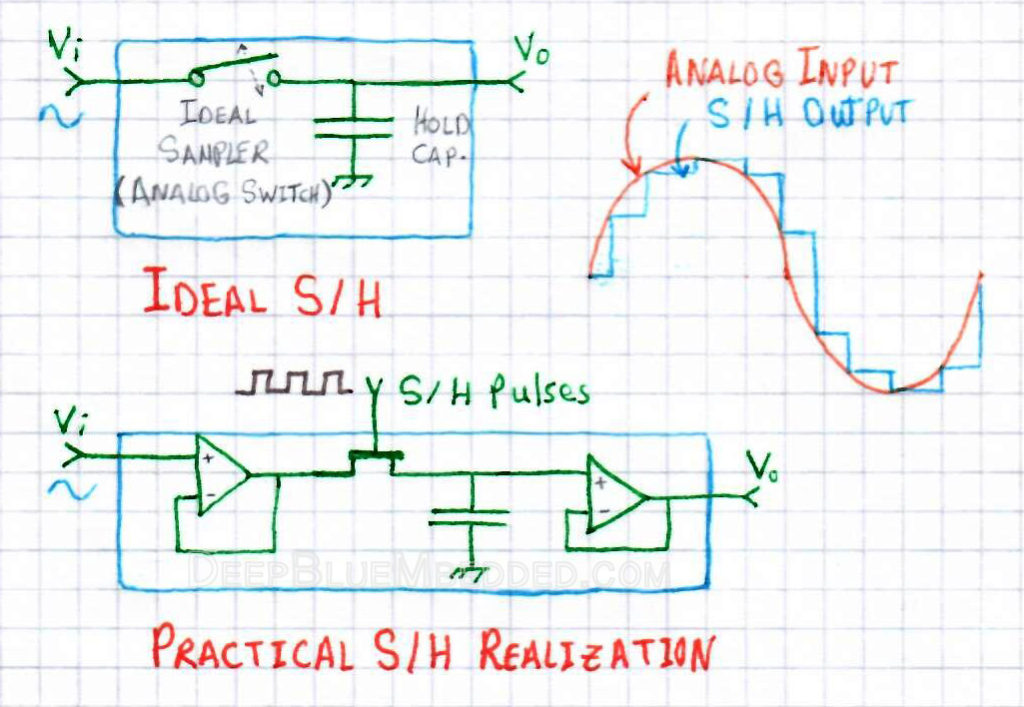
ADC Sampling
The Analog input signal which is a continuous function in time has to be held constant for a short period of time during which the ADC can convert the instantaneous value to its digital representation. This process is done by the Sample/Hold circuitry which is basically an Analog Switch + a Holding Capacitor. It can get more complicated in advanced converters but we’re assuming the very basic S/H circuitry.
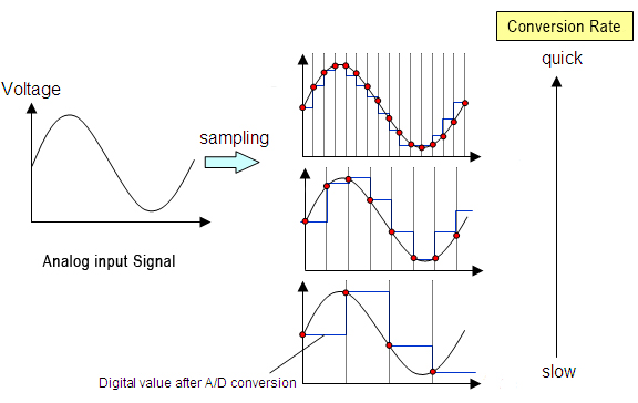
Sampling Rate
The rate at which an ADC converts the continuous analog signal to digital data is called “Sampling Rate”. And if it takes Ts time to convert a single sample, then the sampling rate of this ADC is Fs = 1/Ts. Then the original analog signal can be reproduced from the discrete-time digital values by mathematical interpolation. The accuracy in this procedure is dictated by the combined effect of the sampling rate and quantization error.
Sampling Theorem
Theoretically, and to get the minimal information about the original analog signal, an ADC must sample and convert the analog signal with a frequency of Fs >= 2FMAX Which satisfies the Shannon-Nyquist sampling theorem.
Fs -> The Sampling Frequency of an ADC
FMAX -> The Maximum Frequency In The Analog Signal Being Converted
Violating this rule will lead to further problems and loss of significant information about the signal. It’s near to impossible to get an idea of what does the original signal look like before conversion. That’s why we practically pick an ADC with a sampling rate (Fs) of about 10 x FMAX To avoid operating near to the fundamental limitations of the sampling.
Over-Sampling
Analog signals are usually sampled at the minimum allowable frequency for economical reasons. However, if an analog signal is sampled at a much higher rate than the Nyquist limitation and then got filtered by a digital filter to limit its bandwidth, we’ll have many interesting results “Achievements in fact”. For example, a 20-bit ADC can be made to act as a 24-bit ADC with 256× oversampling.
The over-sampling technique is typically used in audio frequency ADCs where the required sampling rate (typically 44.1kHz) is very low compared to the clock speed of typical logic circuits (>1MHz). In this case, by using the extra bandwidth to distribute quantization error onto out of band frequencies, the accuracy of the ADC can be greatly increased at no additional cost.
ADC Resolution & Quantization
Resolution
The Resolution of an ADC indicates the number of discrete values it can produce over the range of analog values. The Resolution also determines the magnitude of the quantization error and therefore determines the maximum possible average signal-to-noise ratio (SNR) for a typical ADC.
The resolution Q depends on both the number of bits n generated by the quantizer and also the FSR (full-scale range) for the analog reference voltage line. Here is the formula to calculate the resolution of quantization Q which is basically a division for the FSR voltage by the number of levels 2n
![]()
Which means, an 8-Bit ADC with an analog reference Vref+of 5v has a resolution of
![]()
That’s why you can potentially increase the ADC conversion resolution by decreasing the analog voltage reference provided that you’re measuring small signals. Alternatively, you can amplify small signals like audio sound captured by a microphone which is typically in milli-volts range.
Quantization
The quantizer circuit is the working horse of an ADC. Its function is to convert the analog voltage captured by the S/H circuitry to the digital corresponding value. There are many schemes for creating a quantization circuit which also determines the type of an ADC. What you should really know in the meantime, that the quantization process whether it’s rounding-off or truncating intermediate analog signals which lie between two Q levels.
Quantization Error
The quantization error is due to the fact that analog signals will always lie between two distinct Q levels. Should we round-off or truncate? doing either will generate what we call “The Quantization Error”. And it can’t be avoided, However, we can improve the overall accuracy using different techniques.
The Signal To Quantization Noise Ratio (SQNR) is calculated using the following formula

![]()
There are many different schemes used by different types of ADCs for analog signal quantization. Hence, we have a variety of ADC types which we’ll be discussing hereafter. Most of which use analog comparators alongside a digital counter, analog integrator, or a D/A in order to achieve the Analog To Digital conversion.
Different Types of ADC
There are many types for Analog To Digital Converters depending on the way they work. Here I’ll list some of the most commonly used ones whether for standalone ADC ICs or being integrated within microcontrollers. You can definitely research for whichever seems interesting to you as this is not going to be a heavily detailed demonstration.
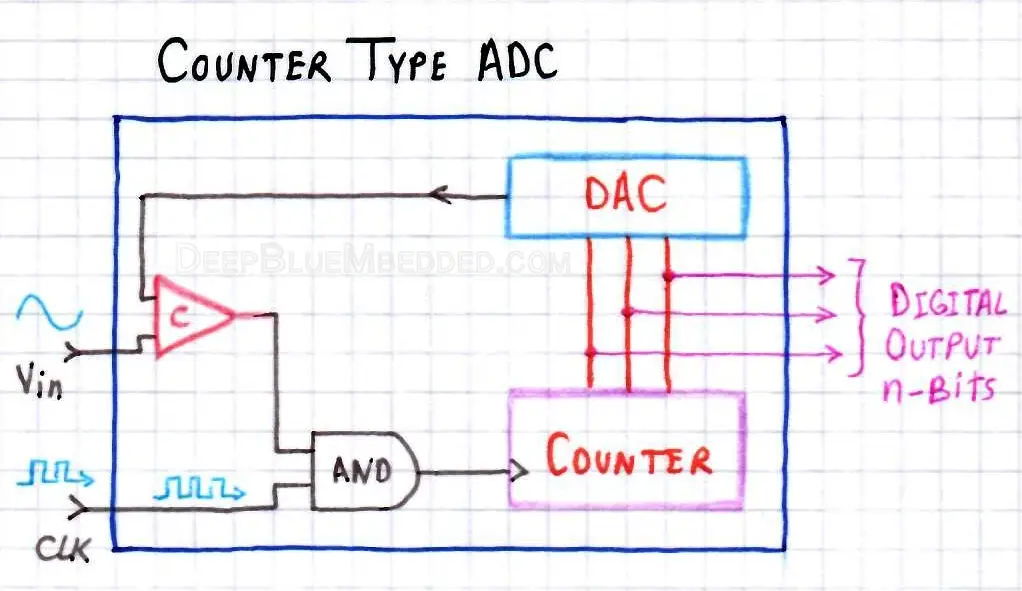
Counter Type ADC
This type of ADC utilizes a DAC (Digital To Analog Converter) in order to perform a quick sweep for the output voltage up to the point where the analog comparator confirms that the output voltage is nearly equal to the analog input signal being measured. Therefore, the counter stops sweeping and its current value is the direct digital representation for the input signal.
The block diagram down below indicates how a Counter Type ADC works
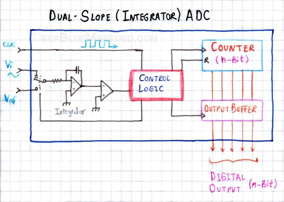
Integrating (Dual-Slope) ADC
An integrating ADC (dual-slope ADC) applies the analog input voltage to the input of an integrator and allows the voltage to ramp for a fixed time period (the run-up period). Then a known reference voltage of opposite polarity is applied to the integrator and is allowed to ramp until the integrator output returns to zero (the run-down period).
The input voltage is computed as a function of the reference voltage, the constant run-up time period, and the measured run-down time period. The run-down time measurement is usually made in units of the converter’s clock, so longer integration times allow for higher resolutions.
The block diagram indicating the functionality of Dual-Slope (Integrating) ADC is shown below.
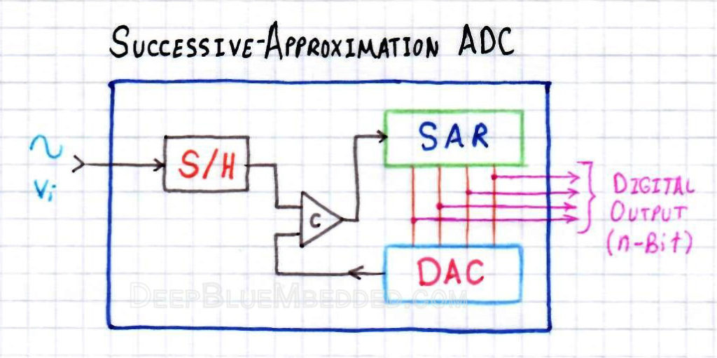
Successive Approximation
The Successive Approximation ADC uses a comparator to successively narrow a range that contains the analog input voltage. At each successive step, the converter compares the input voltage to the output of an internal DAC which might represent the midpoint of a selected voltage range. At each step in this process, the approximation is stored in the successive approximation register (SAR).
The block diagram indicating the functionality of Successive Approximation ADC is shown below.
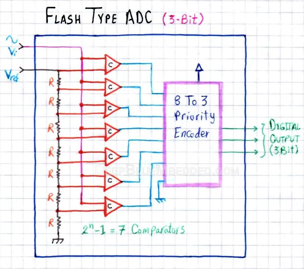
Flash Type ADC (Direct)
The Flash type ADC consists of (2n-1) parallel analog comparators. These comparators are sampling the analog input signal in parallel and driving the logic circuit which generates the digital code for each voltage level. It’s also called direct conversion as it’s the fastest type of ADC at all.
However, it’s limited in resolution. Typically 8-Bits are being used commonly, as increasing the resolution by a single 1 bit will require twice the number of comparators being used. And therefore, it’s extremely expensive and has a large size.
The block diagram indicating the functionality of Flash Type ADC (3-Bit) is shown below.
ADC Module in PIC Microcontroller
For the rest of this tutorial, we’ll discuss the ADC Module in PIC16F microcontrollers. How it works and how to configure and use it to read analog channels for our projects.
Hardware Description
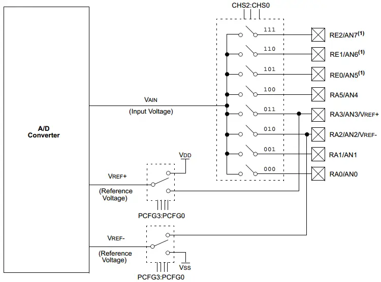
The Analog-to-Digital (A/D) Converter module has 5-Channels for the 28-pin devices and 8-Channels for the 40/44-pin devices. The conversion of an analog input signal results in a corresponding 10-Bit digital number.
The A/D module has high and low-voltage reference input that is software selectable to some combination of VDD, VSS, RA2 or RA3.
The A/D converter has a unique feature of being able to operate while the device is in Sleep mode. To operate in Sleep, the A/D clock must be derived from the A/D’s internal RC oscillator.
Block Diagram
Here is the block diagram for the A/D converter in out PIC16F877A microcontroller.
ADC Special Function Registers
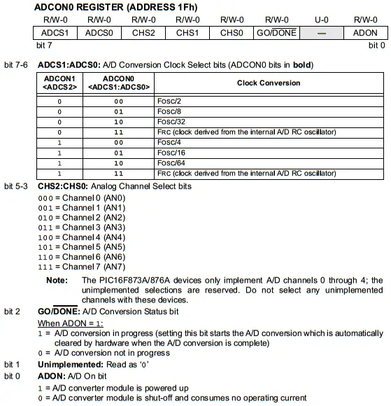
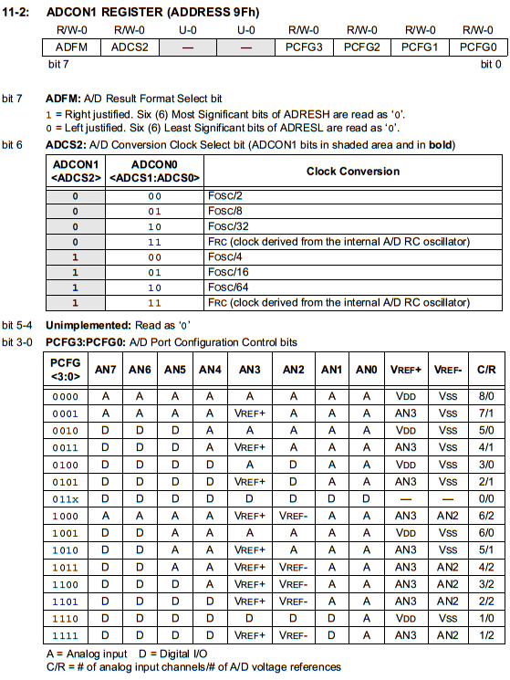
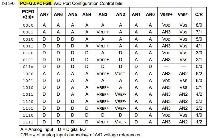
The A/D module has four registers. These registers are
- A/D Result High Register (ADRESH)
- A/D Result Low Register (ADRESL)
- A/D Control Register 0 (ADCON0)
- A/D Control Register 1 (ADCON1)
The A/D conversion 10-Bit result is stored in (ADRESH+ADRESL) registers.
The operation of the ADC module is completely controlled by (ADCON0+ADCON1) registers.
ADCON0 Register
ADCON1
Analog Reference
The A/D module has high and low-voltage reference input that is software selectable to some combination of VDD, VSS, RA2 or RA3. You can select the voltage references in the same way as analog channel selection using the table above.
Let’s assume a Vref+ of VDD = 5v and Vref– of Vss = 0v for this tutorial. Which results in a full-scale range (FSR) of 5v. Therefore, the A/D conversion resolution will be
![]()
Channel Selection
In our microcontroller’s ADC module, there are 8 Analog Channels. These channels are multiplexed to a single 1 A/D converter, that’s why an analog switch exists in the block diagram. And you, the programmer, has to select the desired channel before an A/D conversion is initiated.
The ADCON1 and TRIS registers control the operation of the A/D port pins. The port pins that are desired as analog inputs must have their corresponding TRIS bits set (input). If the TRIS bit is cleared (output), the digital output level (VOH or VOL) will be converted. The A/D operation is independent of the state of the (CHS2:CHS0) bits and the TRIS bits.
A/D Aquisition Time
After the A/D module has been configured as desired, the analog signal of the selected channel must be acquired before the conversion is started. The analog input channels must have their corresponding TRIS bits selected as inputs. After this acquisition time has elapsed, the A/D conversion can start.
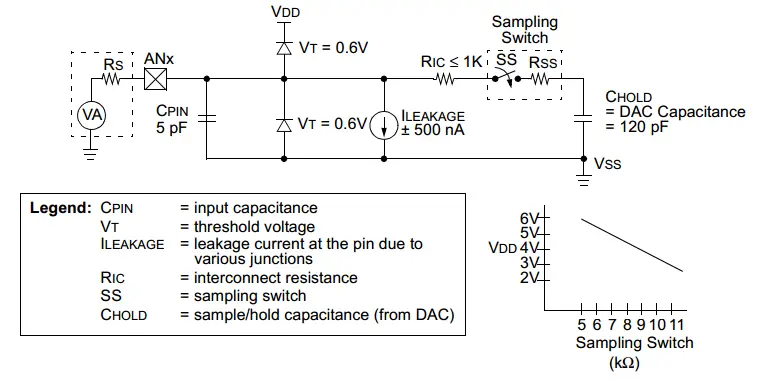
For the A/D converter to meet its specified accuracy, the charge holding capacitor (CHOLD) must be allowed to fully charge to the input channel voltage level.
The maximum recommended impedance for analog sources is 2.5 kΩ. As the impedance is decreased, the acquisition time may be decreased. After the analog input channel is selected (changed), this acquisition must be done before the conversion can be started.
To calculate the minimum acquisition time TACQ, you can use the equation below. This equation assumes that 1/2 LSB error is used (1024 steps for the A/D). The 1/2 LSB error is the maximum error allowed for the A/D to meet its specified resolution.
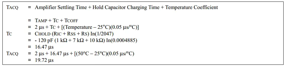
This equation is derived depending on the analog input model circuitry in the diagram below. And you can optimize your system for much lower acquisition time by a little bit more investigation in this model. Alternatively, you can shoot for a safe value instead.
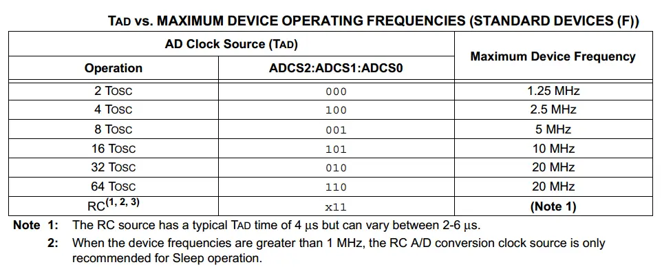
A/D Conversion Clock Selection
The A/D conversion time per bit is defined as TAD. The A/D conversion requires a minimum of 12 TAD per 10-bit conversion. The source of the A/D conversion clock is software selected. The seven possible options for TAD are:
- 2 TOSC
- 4 TOSC
- 8 TOSC
- 16 TOSC
- 32 TOSC
- 64 TOSC
- Internal A/D module RC oscillator (2-6 µs)
For correct A/D conversions, the A/D conversion clock (TAD) must be selected to ensure a minimum TAD time of 1.6 µs. The table below shows the resultant TAD times derived from the device operating frequencies and the A/D clock source selected.
Starting A/D Conversion
Setting the GO/DONE bit starts a new conversion for the selected channel. A new conversion should not start before the Aquisition Time TACQ has elapsed.
Clearing the GO/DONE bit during a conversion will abort the current conversion. The A/D Result register pair will NOT be updated with the partially completed A/D conversion sample. That is, the (ADRESH:ADRESL) registers will continue to contain the value of the last completed conversion (or the last value written to the ADRESH:ADRESL registers). After the A/D conversion is aborted, the next acquisition on the selected channel is automatically started. The GO/DONE bit can then be set to start the conversion.
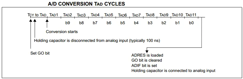
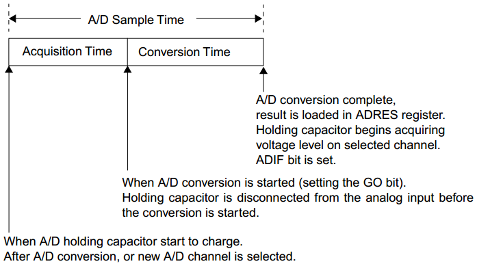
The figure below indicates the A/D conversion cycles that it takes to convert an analog signal since setting the GO/DONE bit until the result is written to the ADRES registers. Also note that after the GO bit is set, the first time segment has a minimum of TCY and a maximum of TAD.
A/D Conversion Sequence Timing
The following diagram will show you the A/D conversion sequence and will also indicate the timing terminology. The acquisition time TACQ is the time that the A/D module’s holding capacitor is connected to the external voltage level.
Then there is the conversion time TC of 10 TAD, which is started when the GO bit is set. The sum of these two times is the sampling time TS. Hence, the sampling frequency FS = 1 / TS.
There is a minimum acquisition time to ensure that the holding capacitor is charged to a level that will give the desired accuracy for the A/D conversion.
A/D Conversion Result Registers
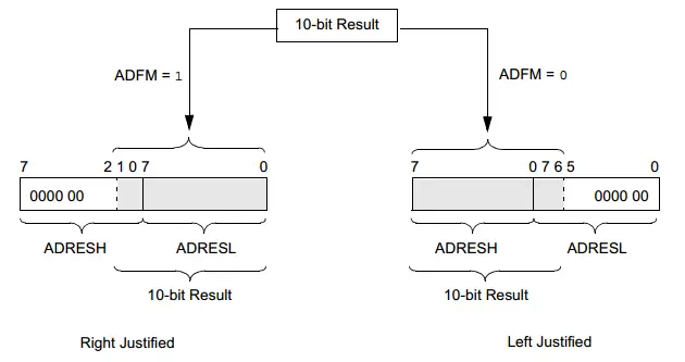
The (ADRESH:ADRESL) register pair is the location where the 10-bit A/D result is loaded at the completion of the A/D conversion. This register pair is 16 bits wide. The A/D module gives the flexibility to left or right justify the 10-bit result in the 16-bit result register.
The A/D Format Select bit (ADFM) controls this justification. The figure below shows the operation of the A/D result justification. Where the extra bits are loaded with ‘0’s.
Maximum Sampling Rate
Maximizing the sampling rate of your ADC is obviously a hard task to go for. However, in some situations, you’ll actually need to get as many samples as you can out of your ADC. So, here are a few things to consider.
Analog channel switching requires additional wait time “Aquisition Time TACQ“. So, if all that you need is a single channel, then you can save so much time as there is no need to switch between channels and unnecessarily waste so much time waiting for CHOLD to charge each time.
Another thing, you can sacrifice the accuracy of your ADC conversion reading for pushing the maximum sampling rate a little bit further.
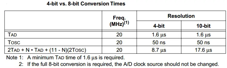
The A/D converter allows you to make the trade-off of conversion speed to resolution. Regardless of the resolution required, the acquisition time is the same. To speed up the conversion, the clock source of the A/D module may be switched so that the TAD time violates the minimum specified time (Shown previously, TADmin = 1.6µs).
Once the TAD time violates the minimum specified time, all the following A/D result bits are not valid. The clock sources may only be switched between the FOSC derived options (cannot be switched from/to RC). The equation to determine the time before the oscillator can be switched is as follows:
Conversion time TC = TAD + N • TAD + (11 – N)(2TOSC)
Where N = number of bits of resolution required
Since the TAD is based on the device oscillator, you must use a method (a timer, software loop, etc.) to determine when the A/D oscillator may be changed.
The following example in the table below shows a comparison of time required for a conversion with 4-bits of resolution, versus the 10-bit resolution conversion. The example is for devices operating at 20MHz (The A/D clock is programmed for 32TOSC) and assumes that immediately after 6TAD, the A/D clock is programmed for 2TOSC. The 2TOSC violates the minimum TAD time since the last 4 bits will not be converted to correct values. And that’s the trick for speeding it up!
Configuring ADC With PIC MCU
Steps To Configure The ADC Module
To do an A/D Conversion, Follow these steps:
1. Configure the A/D module
• Configure analog pins/voltage reference and digital I/O (ADCON1)
• Select A/D input channel (ADCON0)
• Select A/D conversion clock (ADCON0)
• Turn on A/D module (ADCON0)
2. Configure A/D interrupt (if desired):
• Clear ADIF bit
• Set ADIE bit
• Set PEIE bit
• Set GIE bit
3. Wait the required acquisition time.
4. Start conversion
• Set GO/DONE bit (ADCON0)
5. Wait for A/D conversion to complete by either:
• Polling for the GO/DONE bit to be cleared (interrupts disabled); OR
• Waiting for the A/D interrupt
6. Read A/D Result register pair (ADRESH:ADRESL), clear bit ADIF if required.
7. For the next conversion, go to step 1 or step 2 as required. The A/D conversion time per bit is defined as TAD.
Implementing Simple ADC Driver
Step1 Configure The ADC Module
All Analog Channels Are Activated, Vref+ = Vdd, Vref- = Vss
Our Fosc = 4MHz, so we’ll choose the ADC clock to be FOSC/8, so 8TOSC = 2μs. Which satisfies the condition of TAD must be larger than 1.6μs.
And finally, Turn ON the ADC module
|
ADCON0 = 0x41; // Turn ADC ON, Select AN0 Channel, ADC Clock = Fosc/8 |
Let’s set the A/D conversion result justification to be “Right-Justified”
Let’s select AN0 channel for example
|
ADCON1 = 0x80; // All 8 Channels Are Analog, Result is «Right-Justified» // ADC Clock = Fosc/8 |
Step2 Configure A/D interrupts (if desired)
|
ADIF = 0; // Clear ADC Interrupt Flag ADIE = 1; // ADC Interrupt Enable Bit PEIE = 1; // Peripherals Interrupt Enable Bit GIE = 1; // Global Interrupts Enable Bit |
Step3 Wait The Required Aquisition Time TACQ
|
__delay_us(30); // The Minimum Tacq = 20us, So That should be enough |
Step4 Start The A/D Conversion
|
GO_DONE = 1; // Start A/D Conversion |
Step5 Wait for A/D conversion to complete by either
1. Polling The GO/DONE Bit
|
while(ADCON0bits.GO_DONE); // Polling GO_DONE = Delay Until Conversion Is Complete // Now You Can Read ADRESH, ADRESL |
2. Respond To The Interrupt Signal!
Alternatively, if you’re using interrupts, you’ll have to do the following
|
void __interrupt() ISR(void) { if(ADIF) { // Read A/D Conversion Result Registers ADRESH, ADRESL // Clear The ADC Interrupt Flag Bit ADIF = 0; } } |
Step6 Read A/D Result register pair (ADRESH:ADRESL)
|
uint16_t AN0_RES = (ADRESH << 8) + ADRESL; // Read The Right-Justified 10-Bit Result |
LED Dimmer – ADC LAB1
| Lab Name | Analog Input – Analog Output (LED Dimmer) – ADC+PWM |
| Lab Number | 21 |
| Lab Level | Beginner |
| Lab Objectives | Learn how to configure The ADC Module and read analog signals. Combine the analog readings from a potentiometer with PWM to control LED brightness. |
1. Coding
Open the MPLAB IDE and create a new project name it “ADC_LED_Dimmer”. If you have some issues doing so, you can always refer to the previous tutorial using the link below.

Set the configuration bits to match the generic setting which we’ve stated earlier. And if you also find troubles creating this file, you can always refer to the previous tutorial using the link below.
Now, open the main.c file and let’s start developing the firmware for our project.
The first task is to initialize the ADC and PWM modules using the basic firmware drivers which we’ve already built previously. Then, we’ll read convert the voltage level on Analog Channel 0 and send the 10-Bit A/D conversion result as a Duty Cycle for PWM1. So the brightness of the LED is determined by the analog input for Channel 0.
Here is the Full Code Listing For This LAB
|
1 2 3 4 5 6 7 8 9 10 11 12 13 14 15 16 17 18 19 20 21 22 23 24 25 26 27 28 29 30 31 32 33 34 35 36 37 38 39 40 41 42 43 44 45 46 47 48 49 50 51 52 53 54 55 56 57 58 59 60 61 62 63 64 65 66 67 68 69 70 71 72 73 74 75 76 77 |
/* * LAB Name: ADC LED Dimer * LAB Num.: 21 * Author: Khaled Magdy * Visit My Website @ DeepBlueMbedded.com */ #include <xc.h> #include «config.h» #include <stdint.h> #define _XTAL_FREQ 4000000 //——[ Prototypes ]—- void PWM1_Init(); void PWM1_Set_Duty(uint16_t); void ADC_Init(); uint16_t ADC_Read(uint8_t); //==================================================== //———-[Main Routine]————- void main(void) { PWM1_Init(); ADC_Init(); while(1) { PWM1_Set_Duty(ADC_Read(0)); // Set PWM Duty Cycle To AN0_Result! __delay_ms(1); } return; } //———-[END OF MAIN]————- //==================================================== //————[ CCP/PWM Routines ]————— void PWM1_Init() { //—[ Configure The CCP Module For PWM Mode ]— CCP1M3 = 1; CCP1M2 = 1; TRISC2 = 0; // The CCP1 Output Pin (PWM) // Set The PWM Frequency (5kHz) PR2 = 124; // Set The PS For Timer2 (1:4 Ratio) T2CKPS0 = 1; T2CKPS1 = 0; // Start CCP1 PWM ! TMR2ON = 1; } void PWM1_Set_Duty(uint16_t DC) { // Check The DC Value To Make Sure it’s Within 10-Bit Range if(DC<1024) { CCP1Y = DC & 1; CCP1X = DC & 2; CCPR1L = DC >> 2; } } //————[ AD Converter Routines ]————— void ADC_Init() { ADCON0 = 0x41; // Turn ADC ON, Select AN0 Channel, ADC Clock = Fosc/8 ADCON1 = 0x80; // All 8 Channels Are Analog, Result is «Right-Justified» // ADC Clock = Fosc/8 } uint16_t ADC_Read(uint8_t ANC) { if(ANC<0 || ANC>7) // Check Channel Number Validity { return 0;} ADCON0 &= 0b11000101; // Clear The Channel Selection Bits ADCON0 |= ANC<<3; // Select The Required Channel (ANC) // Wait The Aquisition Time __delay_us(30); // The Minimum Tacq = 20us, So That should be enough GO_DONE = 1; // Start A/D Conversion while(ADCON0bits.GO_DONE); // Polling GO_DONE Bit // Provides Delay Until Conversion Is Complete return ((ADRESH << 8) + ADRESL); // Return The Right-Justified 10-Bit Result } |
2. Simulation
Here is an animation for the running simulation tests.
3. Prototyping
Wiring up this schematic on a breadboard should be an easy task. Just upload your firmware hex file to the microcontroller chip. And hook up the input power rails and start testing it up!
Here is a video for the final output of this LAB.
If you’ve any troubles or got stuck at any point, just drop me a comment. I’ll be always here and ready for help. Or even other readers may do a better job in this.
Download LAB Project
Finger Snap Switch – ADC LAB2
| Lab Name | Finger Snap Switch |
| Lab Number | 22 |
| Lab Level | Intermediate |
| Lab Objectives | Learn how to configure The ADC module and read analog signals. Identify sound intensity (loudness) in order to flip a LED when a finger snap is captured by a microphone! |
1. Coding
Open the MPLAB IDE and create a new project name it “ADC_Microphone”. If you have some issues doing so, you can always refer to the previous tutorial using the link below.
Set the configuration bits to match the generic setting which we’ve stated earlier. And if you also find troubles creating this file, you can always refer to the previous tutorial using the link below.
Now, open the main.c file and let’s start developing the firmware for our project.
The first task is to initialize the ADC module using the basic firmware driver which we’ve already built previously. Then, we’ll continuously convert & read the voltage level on Analog Channel 0 (The Microphone Amplified Output) and compare 10-Bit A/D conversion against a specific threshold value. So we can detect any loud sound nearby and flip an LED as a result.
Here is The Full Code Listing For This Project
|
1 2 3 4 5 6 7 8 9 10 11 12 13 14 15 16 17 18 19 20 21 22 23 24 25 26 27 28 29 30 31 32 33 34 35 36 37 38 39 40 41 42 43 44 45 46 47 48 49 50 51 52 53 54 55 56 57 58 59 |
/* * LAB Name: ADC Microphone (Finger Snap Switch) * LAB Num.: 22 * Author: Khaled Magdy * Visit My Website @ DeepBlueMbedded.com */ #include <xc.h> #include «config.h» #include <stdint.h> #define _XTAL_FREQ 4000000 //——[ Prototypes ]—- void ADC_Init(); uint16_t ADC_Read(uint8_t); //==================================================== //———-[Main Routine]————- void main(void) { uint16_t AN0_RES = 0, TH = 850; // You’ll Have To Figure Out // The Best Threshold Value For You ADC_Init(); // Initialize ADC Module TRISC7=0; // IO Output Pin (LED) RC7=0; // Initially OFF while(1) { AN0_RES = ADC_Read(0); // Read Analog Channel 0 if(AN0_RES > TH) { RC7 = ~RC7; __delay_ms(10); } __delay_ms(1); } return; } //———-[END OF MAIN]————- //==================================================== //————[ AD Converter Routines ]————— void ADC_Init() { ADCON0 = 0x41; // Turn ADC ON, Select AN0 Channel, ADC Clock = Fosc/8 ADCON1 = 0x80; // All 8 Channels Are Analog, Result is «Right-Justified» // ADC Clock = Fosc/8 } uint16_t ADC_Read(uint8_t ANC) { if(ANC<0 || ANC>7) // Check Channel Number Validity { return 0;} ADCON0 &= 0b11000101; // Clear The Channel Selection Bits ADCON0 |= ANC<<3; // Select The Required Channel (ANC) // Wait The Aquisition Time __delay_us(30); // The Minimum Tacq = 20us, So That should be enough GO_DONE = 1; // Start A/D Conversion while(ADCON0bits.GO_DONE); // Polling GO_DONE Bit // Provides Delay Until Conversion Is Complete return ((ADRESH << 8) + ADRESL); // Return The Right-Justified 10-Bit Result } |
Note!
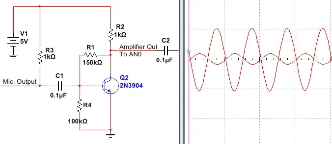
Note: You should know that the output audio signal captured by the microphone will be a few milli-volts in magnitude! That’s almost identical to the resolution of our ADC, therefore it’s impossible to capture such a signal. Hence, we’ll have to build a very basic amplifier to give this signal a constant gain. Here is the simplest common-emitter amplifier that you can build with a transistor and a few resistors.
2. Prototyping
And here is a video for the final output of this LAB.
If you’ve any troubles or got stuck at any point, just drop me a comment. I’ll be always here and ready for help. Or even other readers may do a better job in this.
Download LAB Project
Different Schemes To Read ADC
Single Channel Conversion
1 One Shot
The one-shot scheme of conversion is basically what we’ve done so far in a previous couple of LABs. The A/D converter is activated and ready for conversion, and if you need to convert a specific analog channel, you’ll call the ADC_Read routine. Consequently, the A/D will switch over to the desired analog channel and a conversion process will be initiated until the result is ready.
This scheme can be used for many applications, specifically low power applications. Which requires low sampling rate A/D conversion. You can set up a timer interrupt and initiate A/D conversions as periodic one-shot conversions.
Sometimes, this scheme will not be sufficient by any means. And I confirm that your ADC is capable of more! it can produce a much higher sampling rate if your application needs to.
|
AN_RES = ADC_Read(ANx); // One-Shot A/D Conversion! |
2 Continuous Mode
This mode is an automatic self-triggering continuous series of A/D conversions. In this way, you’ll push your ADC to its limits and go far near the maximum sampling rate possible.
You can set up A/D interrupt and self-trigger the ADC after reading each sample. As you know, switching channels require waiting some time which is something that you don’t want. Provided that your target is to shoot for the maximum possible A/D sampling rate.
To give you an idea of how this can be implemented, here is a code snippet for the ISR in this case
|
void __interrupt() ISR(void) { if(ADIF) { // Read A/D Conversion Result Registers ADRESH, ADRESL AN_RES = (ADRESH << 8) + ADRESL; // Clear The ADC Interrupt Flag Bit ADIF = 0; // Start New Conversion! GO_DONE = 1; } } |
Please, be advised that this scheme maximizes your overall ADC’s sampling rate. However, you should know that you’re sacrificing CPU time which is going to be overloaded by the excessive amount of interrupts. This “interrupts jitter” is obviously proportional to the current sampling rate of your ADC + any other interrupt sources!
Multiple Channels Conversion
1 Burst of Conversions
In some situations, your microcontroller will have to read multiple analog channels. And as we know that there is only 1 A/D resource. That’s why we have to configure the analog channel selection switch before issuing an A/D conversion.
One way to get this task done is to do a burst of conversions in a row for all your analog channels. In this way, you’ll be able to sequentially convert all your channels in a row. Here is a typical implementation for a burst conversion routine.
|
void ADC_Burst(uint16_t* AN_RES_BUF, uint8_t N) { for(uint8_t i = 0; i<N; i++) { ADCON0 &= 0x11000101; // Clear The Channel Selection Bits ADCON0 |= i<<3; // Select The Required Channel (i) // Wait The Aquisition Time __delay_us(30); // The Minimum Tacq = 20us, So That should be enough GO_DONE = 1; // Start A/D Conversion while(ADCON0bits.GO_DONE); // Polling GO_DONE Bit // Provides Delay Until Conversion Is Complete AN_RES_BUF[i] = ((ADRESH << 8) + ADRESL); } } |
2 Continuous Bursts
Obviously, you can set up the A/D converter interrupt signal in order to continuously update your analog channels result buffer sequentially. And the “interrupt jitter” problem will also arise in this case.
1
How To Measure Voltage Greater Than Vcc (>5v)
You can just attenuate the original signal by using a proper attenuator or maybe a voltage divider! a couple of resistors will give your ADC much higher upper limit for conversion.
Using R & R resistors, you’ll make your ADC capable of reading up to 10volts. Similarly, using R & 3R, you’ll be able to read signals up to 20volts. Just Apply Voltage Divider Rule.
What you should notice is the fact that the accuracy is dropping significantly as we go up. The lower the voltage is, the less error generated by the A/D measurement setup.
2
How To Measure Small Signals (~mv)
Designing a suitable amplifier for your system will make the job of A/D converter much easier. Sometimes a simple common emitter amplifier will do the trick. Even an op-amp can do much help.
However, sometimes you may need something different. Here is an example, instead of trying to measure too very small signals to check the difference between them. You just can use a differential amplifier and amplify this difference between the signals. Now the job of our ADC is much easier than before! And so on…
3
Converting ADC Result Back To Voltage
After a successful A/D conversion, you can work it in reverse to calculate back the original voltage level. This only requires the knowledge of your ADC’s current resolution Q.
For 10-Bit ADC with FSR=5v, assume a digital result of conversion ANRES = 256
Then the analog corresponding voltage is calculated as shown below
![]()
![]()
Was this helpful for you? Why not share it with your network! it took too much time and effort in order to craft such a piece of content. Sharing is the best way for supporting free technical content like this,
Regards,
Khaled M.
| Previous Tutorial | Tutorial 22 | Next Tutorial |