Содержание
- ERROR:Pack:1654 — The timing-driven placement phase encountered an error
- venky.817
- ads_ee
- Mesa 7i95
- [SOLVED] Latching issue on storing a value
- dpatel
- dpatel
- TrickyDicky
- XILINX ISE устанавливает маркер ввода-вывода как часы
- Convert an ML505 EDK project for the XUPV5
- Change the target FPGA
- Add the PCIe Bridge Constraints
- Remove the DDR2 constraints
- Add the new DDR2 constraints
- Build the project
ERROR:Pack:1654 — The timing-driven placement phase encountered an error
venky.817
Newbie level 3

i am getting this error while executing code in xilinx vlx6365t kit.
ERROR lace:1153 — A clock IOB / BUFGCTRL clock component pair have been found
that are not placed at an optimal clock IOB / BUFGCTRL site pair. The clock
IOB component is placed at site . The corresponding BUFGCTRL
component is placed at site . The clock IO can use
the fast path between the IOB and the Clock Buffer if a) the IOB is placed on
a Global Clock Capable IOB site that has the fastest dedicated path to all
BUFGCTRL sites, or b) the IOB is placed on a Local Clock Capable IOB site
that has dedicated fast path to BUFGCTRL sites in its half of the device (TOP
or BOTTOM). You may want to analyze why this problem exists and correct it.
If this sub optimal condition is acceptable for this design, you may use the
CLOCK_DEDICATED_ROUTE constraint in the .ucf file to demote this message to a
WARNING and allow your design to continue. However, the use of this override
is highly discouraged as it may lead to very poor timing results. It is
recommended that this error condition be corrected in the design. A list of
all the COMP.PINs used in this clock placement rule is listed below. These
examples can be used directly in the .ucf file to override this clock rule.
ERROR ack:1654 — The timing-driven placement phase encountered an error.

ads_ee
Full Member level 6

This occurs when you have a clock input that needs to traverse from one I/O bank into a second I/O bank to say reach a MMCM or in your case a BUFGCTRL. I recall for V6 this is allowed if using a MRCC clock input but not with an SRCC clock input.
Without knowing what pins/MMCM/BUFG you are using in your design I can’t tell you specifically what is the problem.
If the crossing of the clock into another bank was intentional then either make sure the clock is on an MRCC clock pin and that the clock is restricted to the bank in comes in on and the adjacent banks above and below that bank. You can also set the CLOCK_DEDICATED_ROUTE to BACKBONE (I think that’s the term). This will allow the clock to reach any MMCM or BUFG in the part, but the tools won’t compensate for the insertion delays in this case.
Источник
Mesa 7i95
- Posts: 14617
- Thank you received: 3581
Please Log in or Create an account to join the conversation.
- Posts: 116
- Thank you received: 33
Thanks Peter. The PIN_7I95D_58 file worked. I should be able to modify this to get my PWMgen.
The PIN_7I95_7I76D_58 file was giving an error very late in the process.
ERROR:Pack:1654 — The timing-driven placement phase encountered an error.
WARNING:ProjectMgmt — File /home/ise/Downloads/hostmot2/TopEthernetHostMot2_map.ncd is missing.
Please Log in or Create an account to join the conversation.
- Posts: 14617
- Thank you received: 3581
Please Log in or Create an account to join the conversation.
- sdwyer
- Offline
- New Member


- Posts: 12
- Thank you received: 0
I’m trying to get my 7i95 card working with a fresh setup. I’m new to LinuxCNC and Mesa, but not new to Linux.
I’m running completely fresh installation Debian Buster amd64 with the preempt rt kernel.
I’ve used git to get the master branch, downloaded the zip mentioned before and put it in place as instructed.
I’ve compiled and run-in-place LinuxCNC — the axis UI sim works.
When i try to pncconf it complains I have no hostmot2 firmware in /lib/firmware/hm2.
If i ignore the warning and continue on, I see options to choose a number of boards with the suffix «-Internal Data» (presumably because of the previous warning). 7i95 is not there.
I’ve spent the last 2 days searching around for information and find fragments of information here and there talking about hm2 firmware, packages, etc. Of note, this post that seems to be a discussion about documenting a ‘recommended’ way to get firmware on later distributions:
In any case, I’m stuck. What have I missed?
Please Log in or Create an account to join the conversation.
- Posts: 14617
- Thank you received: 3581
1. If you use current master, you dont need any additional zip files, LinuxCNC master now supports the 7I95.
2. There is currently no pncconf support for the 7I95 but you could use a 7I96 configuration
file set if you replace all occurrences of ‘7i96’ with 7i95. You would also have to edit any input pin
connections to use the 7I95s different input pin names.
Please Log in or Create an account to join the conversation.
- sdwyer
- Offline
- New Member
- Posts: 12
- Thank you received: 0
thanks! I’ll give it a try.
Please Log in or Create an account to join the conversation.
- sdwyer
- Offline
- New Member
- Posts: 12
- Thank you received: 0
Thanks for your help. I’ve had success getting the 7i95 board working with the latest head branch from git.
I’m mapping out all my pins in HAL to make things work now.
I’m looking at spindle control. From what I’m reading, it sounds like I need to somehow re-purpose one of the stepper outputs to generate a PWM signal for spindle control. I also need a 3 more very low power (
5mA@5V) single ended outputs for CW/CCW direction and an enable signal.
I’d like to preserve the SSR outputs for switching coolant, lube, etc if thats possible. Seems a waste for SSRs to be doing such light duty.
I also intend to put an encoder on the spindle for rigid tapping, so I’m assuming the 6th encoder input can just be used as-is for this?
Whats the best way to achieve this? Does it require customised firmware or parameters when I ‘loadrt hm2_eth . ‘?
Sorry if these are dumb questions — I guess this is the price I pay for being new to LinuxCNC, Mesa, and picking a card to use thats not yet supported by the «stable» version of LinuxCNC.
Please Log in or Create an account to join the conversation.
Источник
[SOLVED] Latching issue on storing a value
dpatel
Newbie level 5

My first post here. I am trying to store a value on a button press:
Now, when I synthesise this it warns of latches on ‘num’ but that’s what I want (to store the value of the switches when the button is pressed). When I try to implement I get an error and can go no further.
I know the latch is because of an incomplete case so if I add an «else» the error goes and everything works.
But this means that when I release the button it will set num back to 0!
What am I doing wrong/missing?

Super Moderator

dpatel
Newbie level 5
OK, sorry for the incomplete info.
num is a std_logic_vector.
The error I get when I ‘implement’ (mapping stage) is
TrickyDicky
Advanced Member level 5
From the looks of it, its trying to make the buttons input a clock, but because its not come in from a clock input, it throws the error above.
Is there any reason you really want latches? any reason you cant use a clock and use the button as the clock enable (and build D types — the much prefered option in FPGAs)
Otherwise you may have to follow the errors advice to covert it to a warning.
Источник
XILINX ISE устанавливает маркер ввода-вывода как часы
Я нахожусь в Xilinx ISE IDE и с помощью редактора схем.
 (нажмите для нового окна)
Файл ограничений выглядит следующим образом:
Но когда я хочу скомпилировать свою программу, возникает такая ошибка:
Как это исправить?
Хотя любой сигнал теоретически может использоваться в качестве часов, это не относится к FPGA; по крайней мере, не оптимально. Часы требуют особых соображений, которые переводят на ограничение, по которому вывод ПЛИС может быть направлен в сеть часов.
Я подозреваю, что в вашем случае вы использовали кнопку для работы в качестве тактового сигнала, который будет работать только на очень маленьком дизайне (например, на вашем) из-за debouncing и того факта, что он не является входным портом с поддержкой тактовой синхронизации.
Вы можете указать инструменту, что вы хотите, чтобы субоптимальный и потенциально ошибочный такт, добавив следующее ограничение на ваш.ucf:
Имейте в виду, что вы не должны этого делать, не будучи уверенным, что ваш дизайн в порядке с ним. Я рекомендую вам продолжить дизайн с «настоящими» часами, подключенными к порту синхронизации на вашей FPGA, на каждой плате есть одна. Это ограничение сделает вашу работу дизайном, но в более крупном, более быстром дизайне, вероятно, будет источником проблем.
Источник
Convert an ML505 EDK project for the XUPV5
For some reason, the Base System Builder in EDK doesn’t support the XUPV5 board so when making an EDK project for the XUPV5 we have to select the ML505 board and modify the project settings later. If you have not yet created an EDK project, you should read the previous post Creating a project using the Base System Builder, and then continue from these instructions.
Change the target FPGA
The ML505 is based on the Virtex-5 XC5VLX50T whereas the XUPV5 is based on the Virtex-5 XC5VLX110T, so the first thing we must do is change the target FPGA of the project.
- Open XPS and open your base project which should have been setup for the ML505 board.
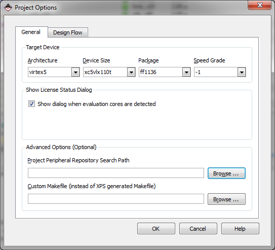
- Select “Project->Project Options”.
- Change the target FPGA setting to “XC5VLX110T”, package “FFG1136” and speed grade “-1”.
- Click “OK” to save the changes.
We’re not finished yet so don’t get too excited and try building the bitstream. If you were to try to build the bitstream, you would come up with this error:
The reason for this error is that the design contains certain location constraints that are optimal for the Virtex-5 XC5VLX50T but not for the XC5VLX110T. We will have to modify the UCF file to use location constraints that are optimal for our FPGA.
Add the PCIe Bridge Constraints
The PCIe bridge peripheral that we included in the project has timing constraints in the project UCF file (system.ucf) but it also has some location constraints in its core specific UCF file (implementation/pcie_bridge_wrapper/pcie_bridge_wrapper.ucf). If you are curious, open this file and read the constraints inside.
The core specific UCF file is generated when you build the project and it is usually generated with constraints that are optimal for the target platform (ie. ML505 in our case). As the ML505 contains a smaller FPGA, the constraints are not optimal for the XUPV5 and we will have to override them by placing the same constraints (with different locations) into the project UCF file (system.ucf).
- Copy and paste the following lines to the bottom of your system.ucf file. Notice that they are the same constraints you would have found in the pcie_bridge_wrapper.ucf file, but I have changed the LOCs. All constraints placed in the system.ucf file will override the core specific constraints.
Remove the DDR2 constraints
The DDR2 memory controller peripheral is the other device with some critical location constraints that we will have to optimize for the XUPV5.
- Find and remove the following lines in the system.ucf file.
Add the new DDR2 constraints
- Add the following constraints to the system.ucf file. You will notice that they are similar to the constraints that we just removed, yes we are replacing the old constraints with these ones!
Build the project
Now you are ready to build the project and if you have done everything right, you should not have any errors.
- Select “Device Configuration->Update Bitstream”. It should take about a half an hour to build depending on your machine.
- You should see the message below if you are successful.
You can download the project files as a compressed zip file here: base-system-xupv5-edk13-1.zip
Источник
Skip to main content
![]()
![]()
Welcome to EDAboard.com
Welcome to our site! EDAboard.com is an international Electronics Discussion Forum focused on EDA software, circuits, schematics, books, theory, papers, asic, pld, 8051, DSP, Network, RF, Analog Design, PCB, Service Manuals… and a whole lot more! To participate you need to register. Registration is free. Click here to register now.
-
Digital Design and Embedded Programming
-
PLD, SPLD, GAL, CPLD, FPGA Design
You should upgrade or use an alternative browser.
ERROR:Pack:1654 — The timing-driven placement phase encountered an error
-
Thread startervenky.817
-
Start dateFeb 13, 2013
- Status
- Not open for further replies.
-
#1
-
#2
Without knowing what pins/MMCM/BUFG you are using in your design I can’t tell you specifically what is the problem.
If the crossing of the clock into another bank was intentional then either make sure the clock is on an MRCC clock pin and that the clock is restricted to the bank in comes in on and the adjacent banks above and below that bank. You can also set the CLOCK_DEDICATED_ROUTE to BACKBONE (I think that’s the term). This will allow the clock to reach any MMCM or BUFG in the part, but the tools won’t compensate for the insertion delays in this case.
- Status
- Not open for further replies.
-
Digital Design and Embedded Programming
-
PLD, SPLD, GAL, CPLD, FPGA Design
-
This site uses cookies to help personalise content, tailor your experience and to keep you logged in if you register.
By continuing to use this site, you are consenting to our use of cookies.
Здравствуйте!
Существует следующая проблема: когда я вставляю Chipscope в дизайн, содержащий bufio2, при компиляции происходит ошибка:
«ERROR:Place:1318 — User has over-constrained component BUFIO2_2CLK_inst_1. There
are no placeable sites that satisfy the user constraints. Please review the
user constraints on the driver component and the load components of
BUFIO2_2CLK_inst_1.
Phase 4.2 Initial Placement for Architecture Specific Features
(Checksum:66d1c629) REAL time: 58 secs
Total REAL time to Placer completion: 58 secs
Total CPU time to Placer completion: 57 secs
ERROR:Pack:1654 — The timing-driven placement phase encountered an error.»
При удалении Чипскопа из дизайна ошибка ичезает. Однако, без использования Чипскопа отладка проекта будет весьма затруднительна. Кто-либо сталкивался с подобного рода проблемой?
Ещё вопрос: можно ли от одного и того же BUFIO2 затактировать ISERDES2, находящиеся в различных полубанках/банках? Если нет, то как это сделать и возможно ли это (цель — подключение ADS5400 к xc6slx150)?
Также, есть ещё одна проблема подобного рода — при вставке блока SelectIO Interface (с использованием соответствующего мастера) проект компилируется. Однако, при подключении UCF с прописанными портами ввода — возникает ошибка:
«Phase 4.2 Initial Placement for Architecture Specific Features
ERROR:Place — ConstraintResolved NO placeable site for
your_instance_name/bufio2_inst
…
ERROR:Place — SIO has over-constrained componet your_instance_name/bufio2_inst
to have to placeable sites. Constraints come from driver constraints AND load
IO constraints
Process «Map» failed»
Если отключить UCF, либо закомментировать все порты ввода (включая тактирование ПЛИС и данных) — компиляция происходит успешно. При этом ISE автоматически назначает порты по своему усмотрению. Но это в данном случае не выход. Можно ли как-то решить данную проблему.
Примеры проектов (2 шт.) по ссылке на файлообменнике:
http://depositfiles.com/files/cn4aixuq0;
http://depositfiles.com/files/4vjbxjowr
Packed loop PLL default input There is an IBUFG unit with a bufg unit in the output, and two bufgs cannot be connected, so this will be reported:
ERROR:NgdBuild:770 — IBUFG ‘u_pll0/clkin1_buf’ and BUFG ‘BUFG_inst’ on net
‘clkin_w’ are lined up in series. Buffers of the same direction cannot be
placed in series.
ERROR:NgdBuild:924 — input pad net ‘clkin_w’ is driving non-buffer primitives:
The following example code:
[Demo1]
 1 // demo1 two bufg connect
 2
 3 module iobuf(
 4
 5    input   clk,
 6
 7    input   rst,
 8
 9    output  led
10
11    );
12
13  wire clkin_w;
14
15  BUFG BUFG_inst(
16
17       .O(clkin_w),           // Clock buffer output
18
19       .I(clk)                   // Clock buffer input
20
21      );
22
23  pll0 u_pll0(
24
25       .CLK_IN1(clkin_w),      // IN
26
27       .CLK_OUT1(clkout),  // OUT
28
29       .RESET(rst));       // IN
30
31 assign led = clkout;
32
33 endmodule
Ordinary IO cannot be directly entered on the locking ring, so this will be reported:
ERROR:Place:1397 — A clock IOB / MMCM clock component pair have been found that
are not placed at an optimal clock IOB / MMCM site pair. The clock IOB
component <clk> is placed at site <A18>. The corresponding MMCM component
<u_pll0/mmcm_adv_inst> is placed at site <MMCME2_ADV_X0Y0>. The clock IO can
use the fast path between the IOB and the MMCM if the IOB is placed on a
Clock Capable IOB site that has dedicated fast path to MMCM sites within the
same clock region. You may want to analyze why this problem exists and
correct it. If this sub optimal condition is acceptable for this design, you
may use the CLOCK_DEDICATED_ROUTE constraint in the .ucf file to demote this
message to a WARNING and allow your design to continue. However, the use of
this override is highly discouraged as it may lead to very poor timing
results. It is recommended that this error condition be corrected in the
design. A list of all the COMP.PINs used in this clock placement rule is
ERROR:Pack:1654 — The timing-driven placement phase encountered an error.
If there is a UCF plus this sentence:
1 NET clk CLOCK_DEDICATED_ROUTE = FALSE;
It will still report an error, in the Zynq7000 series, this is not, as follows:
ERROR:PhysDesignRules:2256 — Unsupported MMCME2_ADV configuration. The signal
u_pll0/clkin1 on the CLKIN1 pin of MMCME2_ADV comp u_pll0/mmcm_adv_inst with
COMPENSATION mode ZHOLD must be driven by a clock capable IOB.
ERROR:Pack:1642 — Errors in physical DRC.
Sample code as follows
[Demo2]
 1 // demo2 regular io directly connect to PLL
 2
 3 module iobuf(
 4
 5     input clk,
 6
 7    input     rst,
 8
 9    output   led
10
11  );
12
13
14
15  pll0 u_pll0(
16
17     .CLK_IN1(clk),      // IN
18
19     .CLK_OUT1(clkout),  // OUT
20
21     .RESET(rst));       // IN
22
23 assign led = clkout;
24
25 endmodule
Use ordinary IO, then connect to bufg to connect to the clock line.
There will be such a mistake, because it is still two bufgs:
ERROR:NgdBuild:770 — IBUFG ‘u_pll0/clkin1_buf’ and BUFG ‘BUFG_inst’ on net
‘clkin_w’ are lined up in series. Buffers of the same direction cannot be
placed in series.
ERROR:NgdBuild:924 — input pad net ‘clkin_w’ is driving non-buffer primitives:
Modify as follows:
[Demo3]
 1 // dem3 regular io with BUFG then connect to PLL which with"No Buffer" setting
 2
 3  module iobuf(
 4
 5    input  clk,
 6
 7    input  rst,
 8
 9    output  led
10
11    );
12
13  wire clkin_w;
14
15  BUFG BUFG_inst (
16
17       .O(clkin_w),           // Clock buffer output
18
19       .I(clk)                   // Clock buffer input
20
21    );
22
23  pll0 u_pll0(
24
25     .CLK_IN1(clkin_w),      // IN
26
27     .CLK_OUT1(clkout),  // OUT
28
29     .RESET(rst));       // IN
30
31 assign led = clkout;
32
33 endmodule
The setting of the PLL is as follows,

Such ordinary IO can be used as a PLL clock input, and the BIT is successfully generated;
The clock is still best to use the global clock IO, you must pay attention when drawing 
There is no concept of Global Clock in ZC702, but there are a lot of dedicated clocks, which are used;
[in conclusion]
No two PLLs are connected in series
Ordinary IO cannot be directly input to the PLL clock input, the dedicated clock tube foot can be;
Ordinary IO can be connected to the PLL clock input by bufg, but to modify the option of the PLL setting INPUT CLK to select «NO BUFFER»;
The specific internal layout allocation can be viewed by Xilinx’s FPGA Editor.
Zynq clock management is also slightly different from the previous film, then in another introduction, related documents <UG472_7Series_Clocking.pdf>